Friday, December 2, 2022

An LCD Retrofit and color display for the Schlumberger SI 4031 Communications Test Set

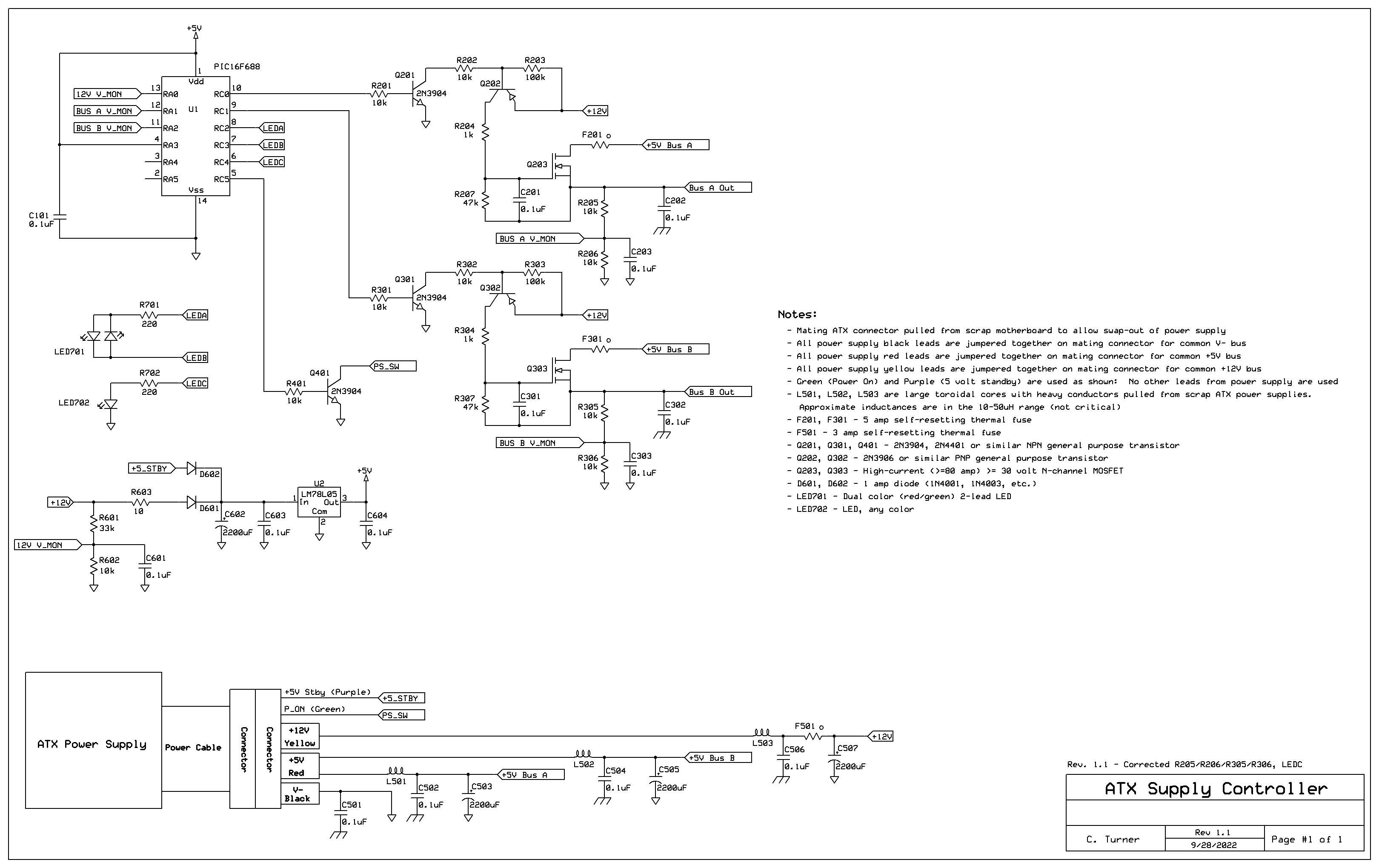
Figure 1: 
The front panel and original green monochrome screen
of the 4031.  A close look shows the "blistering" on the
screen protectors due to delamination, making the
display more difficult to read.
Click on the image for a larger version.
The Schlumberger SI 4031 is a early-mid 1990s vintage communications test set (a.k.a. "Service Monitor") - a device that is designed to test both receivers and transmitters used in the telecommunications industry.  The 4031's frequency range is 400 kHz to 999.9999 MHz making it useful as a general-purpose piece of test equipment, particularly for the testing of amateur radio gear.
Some of its built-in functions include wattmeter, signal generator with modulator for AM, FM and phase-modulated radios, spectrum analyzer, tracking generator and oscilloscope to mention but a few.

As you would expect from a device from the 1990s, the original display used a CRT (Cathode Ray Tube) based monitor operating at something "close" to PAL horizontal and vertical scan rates.  While the CRT monitor in this unit is still in reasonable shape - aside from requiring a "re-cap" (e.g. replacement of electrolytic capacitors) I decided to take on the challenge of putting a more "modern" LCD-type display in it - perhaps taking advantage of a minor savings in both weight and power consumption.

This requires no electrical modification of the 4031 itself and only minor mechanical changes to mount the LCD panel and its related hardware.  (This may also work for the 4032, a version of this unit that covers up to 2 GHz - see below for comments.)

Is it "PAL"

While the pedants would say that a monochrome-only signal cannot be PAL, the reference is, instead, to the horizontal and vertical scan rates of 15.625 kHz and 50 Hz, respectively which are close to those found in the PAL system used in Europe.  As is typical for pieces of non-consumer gear and test equipment, the horizontal and vertical synchronization signals and the video are brought out independently of each other, each being represented as a TTL signal.
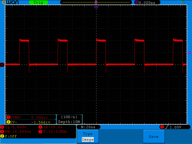
Figure 2:
The horizontal sync pulse train showing 25%
D.C. pulses at 15.625 kHz, TTL level.
Click on the image for a larger version.
The video display generator of the 4031 is interesting in that it uses a UPD7220A graphics controller to facilitate interaction with the CPU (e.g. access memory, produce characters, etc.) but two separate display RAMs (8k x 16 bits) with one being used for access by the UPD7220A and the other, copied from the first during the vertical interval, for pixel read-out - the latter function being done with a combination of "glue logic" and programmable logic devices.

The forgiving nature of the CRT monitor

One nice feature of a CRT monitor is that it can be quite forgiving of deviations from standard video applied to it.  Many - but not all - all-in-one sync decoder chips used in CRT monitors are happy with taking horizontal and vertical signals that are "close" to some standard - but not exact - and lock onto it satisfactorily.  Such is the case with the 4031:  While there are separate horizontal and vertical synchronization signals, neither is quite standard, but it's "close" enough for the old monitor.

Figure 3: 
The vertical sync, showing a 10% duty cycle
pulse at about 50 Hz.
Click on the image for a larger version.

For example, the horizontal synchronization signal is simply an uninterrupted 25% duty cycle pulse train occurring at the horizontal sweep rate of about 15.625 kHz (e.g. 16uSec long) while the vertical synchronization is a 50.08 Hz 10% duty cycle (e.g. 2 msec long) pulse train.  Unlike sync signals found in other applications, the horizontal signal does not contain any sort of blanking (suppression of pulses) during the vertical interval.

Within the 4031's original CRT monitor, the horizontal and vertical synchronization signals are handled completely separately (by a TDA2593 and TDA1170, respectively) so the fact that they are non-standard is irrelevant.

Unfortunately, any modern LCD display device that is expecting a PAL-like signal (in terms of timing) isn't likely to be happy with separate, non-standard synchronization inputs.

Initial attempts:

Initially, I was hoping that an off-the-shelf LCD monitor display like the 7", 4:3 aspect CLAA070MA0ACW with a driver board could be made to work with these signals with no other hardware, but my work was thwarted by the fact that its VGA input - which might handle separate horizontal and vertical sync signals - would not function at PAL video rates - only VGA rates, which have roughly twice the horizontal and vertical frequencies.  While it may have been possible to modify the firmware on this board and re-flash it with one of the "customized" versions found in various corners of the Internet, I chose not to do this.

I then attempted to make a simple analog sync combiner circuit and apply the signal to the composite video input, but found this to be unstable - plus there was the fact that the video display board itself did not have the capability of setting the horizontal and vertical size to fully-fill the screen to the edges, something desirable to make the active screen area fully-fit the window on the front and also align with the buttons along the bottom of the screen.

After a bit more research, I decided to get a GBS-8200 video converter board (Version 4.0), a relatively inexpensive digitizing board designed to convert the myriad of video formats from CRT-based arcade video games and computer inputs to VGA which would then be inputted to a standard monitor and the CLAA070MA0ACW display driver board.  As such, I presumed that it would be far more forgiving to variations from standard video signaling - and I was, fortunately, correct

Sync (re)processor:

While I was originally hopeful that I could simply apply the horizontal and vertical sync inputs to the GBS-8200, the non-standard sync timing (pulse width, lack of a gap of horizontal sync pulses during the vertical interval) did not produce stable results, so a simple circuit had to be devised to modify the sync signal:  This basic circuit is shown below.

Figure 4:
Diagram of the sync processor itself.
This circuit will produce a sync to which the GBS-8200 board can lock.  The single video output
is connected to the RGB input of the GBS-8200 to produce a monochrome (single color)
display as seen in Figure 6.
Click on the image for a larger version.

This circuit works as follows:
 
The horizontal and vertical sync pulses are input to and buffered by sections of a 74HC14, Schmidt-trigger inverters which server to "clean up" the input signals as necessary.  An inverted version of the vertical sync pulse holds U3, a 4017 counter in reset until a vertical interval occurs.

Figure 5:
The circuit in Figure 4 built
on a prototyping board, the
results seen in Figure 6.
Click for a larger image.

During the vertical pulse U3, the counter, is clocked by the horizontal sync pulses and on the 5th count, the timer is stopped, setting the input of U2b, a 4011 NAND gate wired as a simple inverter, high.  U2d is used to "gate" the output of the counter - being only active only when the timer has stopped at the 5th count and during the vertical interval meaning that its output goes high only when the timer is actually counting - not while it's stopped at its terminal count or held in reset. The output of this gate is combined with a "re-inverted" copy of the vertical sync to produce a new version of the vertical sync that is about 225 microseconds long rather than the original 2 milliseconds as depicted in Figure 7 (below).

FWIW, I used the 4011 NAND gate because I found a rail of them in my parts bin - but I couldn't find any 74HC00s at the time which would have worked fine, albeit with a different pin-out.  Similarly, either CMOS CD4017 or 74HC4017 counter would have been fine as well considering the low frequencies present.  I would, however, recommend using only the 74HC14 (or 74HCT14) as it's plenty fast for the video data and it has fairly "strong" outputs (e.g. source/sink currents) as compared to the older and slower CD4069 or 74C14 hex Schmidt inverter.

Note that while it would theoretically be possible to use a one-shot analog timer to generate a new, shorter pulse, doing so would result in visible jitter of the video signal (I tried - it did!) as that timing would neither be consistent or its length precisely synchronous with the horizontal timing:  The use of the horizontal sync to "re-time" the duration of this new vertical pulse assures that the timing of the new pulse is synchronous with both sets of pulses and completely jitter-free.

This new, re-timed vertical sync pulse is then applied to U2a which gates it with the horizontal sync:  The output is then inverted by U1c to produce a composite sync signal (see Figure 7, below) that, while not exactly up to PAL standards, is "close enough" for the GBA-8200 video converter - configured for "RGBS" mode - to be happy.

Elsewhere in the diagram may be seen inverter sections U1d-U1f:  These are configured as buffers to condition the TTL video input and provide a drive signal to the video input of the GBA-8200.

Suitable for a monochrome image!

The circuit in Figure 4 is sufficient, by itself, to drive the GBS-8200 and produce a stable VGA version of the 4031's video signal.

Figure 6:
The monochrome output from the GBS-8200 board using the
sync processor seen in figures 4 and 5 via an external monitor.
Click on the image for a larger version.
The "VID_OUT" signal may be connected to the Red, Green and Blue video inputs of the GBS-8200 and the input potentiometers adjusted for a single color:  White will result if the individual channels' gains are set equally, but green, yellow or any other color is possible by adjustment of these controls.

Figure 6 shows the result of that:  The VGA output from the GBS-8200 was connected to an old 4:3 computer monitor that I had kicking around, producing a beautiful, stable, monochrome signal.

Full-color output from the 4031

The SI 4031's video output is a single TTL signal, meaning that there is not even any brightness information, making it capable of monochrome only.  Fortunately, it is possible to simulate context-sensitive color screens with the addition of a bit of extra circuitry and firmware as described below.

The portion of this circuit used for processing the sync pulses is based on that shown in Figure 4:  A few reassignments of pins were done in the sync re-timer, but the circuit/function is the same.  What is different is the addition of U5, a 74HC4066 quad analog switch and U6, a PIC16F88 microcontroller, and a few other components.

How it works:

The video signal is buffered by U1d-U1f and applied to R1, a 200 ohm potentiometer, the wiper of which is applied to Q1, a unity-gain follower to buffer the somewhat high-impedance video from R1 to something with a source impedance of a few ohms and, more important, constant output with varying load.  The "bottom" end of R1 is connected to U5c, on section of the 74HC4066 which, if enabled, will shunt some of the video signal to ground, reducing its intensity, adjustable via R1.  Via diode D1, this line is also connected to a pin of the microcontroller - the "MARK" pin - more on this later.
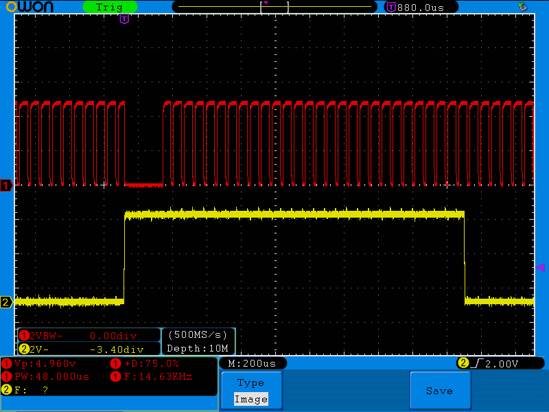
Figure 7:
Top (red) trace: The composite sync from the
circuit of Figures 4 & 8.  Bottom (yellow) trace:
The original vertical sync pulse  for comparison.
Click on the image for a larger version

The output of Q1 is then applied to U5a, U5b and U5d via 100 ohm resistors.  These analog switches will selectively pass the video to the Red, Green or Blue channels of the monitor, depending on microcontroller control.  At the outputs of each of these switches may be found a resistor and diode in series (e.g. D2/R6) and these are connected to output pins of the microcontroller:  If these pins are driven low by the microcontroller, the diode drop and series resistance of the 33 ohm resistor (e.g. R6) and the 100 ohm resistor (e.g. R3) and the output transistor of the microcontroller will shunt some of the voltage and reduce the amplitude on that channel to provide a means of brightness control, increasing the color palette.

I'd originally intended to place emitter-follower video drivers (e.g. the circuit of Q1 in Figure 8) on each of the R, G, and B outputs, but the very short lead length to the input of the GBS-8200 (e.g. no visible signal reflections) - and the ability to adjust the RGB input gain via its three potentiometers - eliminated this requirement as additional losses through the analog switches and other components could be easily compensated.

Figure 8:
Added to the sync processor of Figure 4, above, is a PIC16F88 used to analyze the video from the 4031
and "colorize" the resulting image. 
See the text for information as to how this works.
Click on the image for a larger version.

With the combination of the three 4066 gates, the "!BRITE" pin, and the three "dim" pins (e.g. "!R_DIM", "!G_DIM" and "!B_DIM") over two dozen distinctly different colors and brightness levels may be generated under processor control.

The magic of the microcontroller

U6, a PIC16F88 microcontroller, is clocked at 20 MHz, its fastest rated speed.  Because its job is to operate the four switches comprising U5 - and the three "dim" pins on the video lines - it must "know" a bit about the video signal from the 4031:

  • The "!V_SYNC" pin gets a conditioned sample of vertical sync from the output of U1a:  It is via this signal that the U6 "knows" when the scan restarts at line one.
  • The "!H_SYNC" signal from the output of U1b is applied to pin RB0, which is configured to trigger an interrupt on the falling edge (the beginning) of the horizontal sync.
  • The "!VID" signal is applied to pin RA4, which is the input of Timer 0 within the microcontroller:  This is used to analyze the content of lines of video to determine the specific content as the timer is able to "count" the number of times that the video goes from low to high on these scan lines -  In other words, a sort of "pixel count".

In operation, the start of each horizontal sync pulse triggers an interrupt in the microcontroller.  If this coincides with the start of the vertical interval, the line count is restarted.

Video content analysis:

Figure 9:
Mounted inside the 4031, the sync processor board is on the
far left, the six pins of the ICSP (In Circuit Serial
Programming) connector being easily accessed.  The buttons
and controls for the other two boards are also accessible.
Click on the image for a larger version.

Visual inspection of each of the screens on the 4031 will reveal that they contain unique attributes.  Most obvious is the title of the screen located near the top, but other content may be present midway down the screen - or very near the bottom - which may be used to reliably identify exactly which screen is being displayed, having determined the "pixel count" for certain lines on each of these screens beforehand.

For each subsequent horizontal sync pulse and corresponding interrupt, the count contained within hardware timer 0 is read - and the timer is immediately reset.  For a number of specific scan lines, their unique counts are stored in RAM.

Attention to detail is required!

Determining the pixel count consistently requires a bit of care in the coding.  As mentioned, this count is based on an interrupt-driven routine that reads the content of hardware timer 0 - but this also means that the code must be written in a way that guarantees that the time between the start of the horizontal sync pulse (and subsequent entry into the interrupt service routine) and the read and reset of timer 0 is as consistent as possible, considering the asynchronicity of the timing of this interrupt and the CPU clock.

What this implies is that the reading this timer and its resetting must not only be done in an interrupt, but that it also be the first thing done within the interrupt function prior to any other actions, particularly any conditional instructions that could cause this timing to vary, resulting in inconsistent pixel counts - something that would preclude the use of anything other than a quickly-responding interrupt.  Another implication is that this interrupt may be the only interrupt that is enabled as preemption by another one would surely disrupt our timing.

Immediately following this action is the setting of the color and brightness attributes by ANDing a copy of the current content port/pin registers to remove the brightness/color bits and then ORing that data with the pre-calculated color/brightness bit mask data into those same registers so that any changes in these attributes occur to the left of the visible pixels in the scan line.

A limitation of this hardware/software is that it is likely not possible to satisfactorily set different colors horizontally, along a scan line - it is possible only to change the color of complete scan lines:  To do this would, at a minimum, require extremely precise timing within the interrupt service routine, adding complexity to the code - and it's not certain that satisfactory results would even be possible.   To do it "properly" would certainly require more complicated hardware - possibly including the regeneration of another clock from the horizontal pixel rate - but doing this would be complicated by the fact that the pixel read-out rate is asynchronous with the sync as noted later.

Using the pixel counts:

At the beginning of the vertical interval, outside any interrupts, the previously-determined counts of low-to-high transitions is analyzed via a series of conditional statements and a variable is set indicating the operating "mode" of the 4031.  This "mode" information is then applied to another look-up table to determine the color to be used for that screen.

One complication is that like other analog video, that coming from the 4031 is interlaced meaning that for certain scan lines - particularly those with diagonal elements - that the pixel count may vary for a given scan line.  Unlike "true" video, the sync pulses from the 4031 contain no obvious timing offset (e.g. "serrations" in the sync) to offset by half a line or identify the specific video field, but with an analog monitor, this wasn't really much of an issue as it would simply paint a line on the screen in "about" the right place, anyway.

For most screens, simply looking at pixel counts of between four and six different lines - most of them on lines from 4 to 15 - was enough to uniquely identify a screen, but others - particularly the "Zoom" screens - sometimes require even a greater number of pixel counts and other techniques to reliably and uniquely identify the screen being displayed.

In particular, differentiating between the "SINAD" and "RMS-FLT" Zoom screens was problematic as both resulted in the same pixel counts for all of the lines usable for unique identification:  The only way to detect the difference was due to the fact that for some lines, the pixel count for the "SINAD" screen would vary due to the aforementioned video field differences - or possibly due to interaction between the asynchronicity of the pixel clock, the CPU clock, and the way counts are registered on a counter input without hardware prescaling.  It was the fact that the count of the SINAD screen varied that allowed it to be reliably differentiated from the "RMS-FLT" screen, which had a very consistent pixel count.

Coloration of the screen:

Many screens on the 4031 have different sections.  For many screens, the upper section contains the configured parameters (e.g. frequency, RF signal level, etc.) while the lower portion of the screen shows the measured values or an oscilloscope display:  Simply by knowing which screen type is being displayed and the current line number, those sections can be colored differently from other portions.

Deciding what color to make what is a purely aesthetic choice, so I did what I thought looked good.  Because about two-dozen different colors are possible, I chose the brightest colors for the most commonly-used screen segments, setting these colors by the function to which they were related.

Finally, all screens have, along the bottom, a set of labels for the buttons below the bottom of the screen:  These may be colored separately as well - and I chose gray (a.k.a. "dim white").

Analyzing the video to determine "pixel counts":

When writing the firmware, a few simple tools were included, notably some variables, hard coded at compile time, that would display the pixel counts.  If, for example, one needed to determine the pixel count for line #14, the pixel count display variable would then be loaded with the pixel count for line 14.  For example, the oscilloscope screen capture shows a pixel count capture:  The left-most pulse is 4 units long followed by a single-unit pulse (meaning "10") followed by a 2 unit long pulse with three more pulses - for a pixel count of 13.

Figure 10:
An example of the "pixel" count:  The 4-unit
wide pulse followed by one pulse represents 10
and the 2-unit wide pulse followed by 3 pulses
represent a pixel count of 13 on the selected line.
Click on the image for a larger version.

Another variable may be set to visually identify which scan line is being counted.  When the scan line being counted occurred, the "MARK" pin would be set high causing an on-screen indication of which line was being inspected, offering a "sanity check" and a visual reference to know which line, exactly, was being checked.

During the vertical interval, pin "RB3" would then be strobed with a series of pulses to indicate the pixel count - a "long" pulse lasting four CPU cycles followed by pulses of 1 CPU cycle, each to indicate the "tens" digit (if any) and a shorter pulse of two CPU cycles followed by the requisite number of 1 CPU-cycle pulses to indicate the "ones" digits. 

Using an oscilloscope triggered on the signal on RB3 (pin 9) these pulses could be read visually on the oscilloscope and by switching between the different screens on the 4031, the "pixel count" of this line for the various screens could be determined:  Repeating this for several different scan lines allow unique identification of all screens.  In the event that there is false detection of a mode, this "pixel count" output could also be configured to show the number of the current modes (in a "#define" statement) when they are detected to aid in debugging.

Comments:

In producing this firmware, I have only one version of the 4031 (with Duplex option) available to me.  Different versions of the 4031 - and the 4032 - may have "other" screens not included in the analysis, or slightly different layout/labeling that will foil the analysis of the scan line.
The way the firmware doing the screen analysis is written, if the scan line analysis doesn't find a match to what it already "knows" about it will cause that screen's text to be displayed in the default color of white.

At present this "scan line analysis" can only be done by setting certain variables in the source code and recompiling - but this was made easier by the inclusion of the "ICSP" connector (noted on the diagram in Figure 8 and visible in Figure 9) to allow in-circuit programming, while the unit is operating.  In theory, it may be possible to come up with some sort of user-interactive means of setting individual screens' colors which could be used to set the colors on screens of different firmware versions or with features that I don't have in my 4031, but this would require significantly more work on the firmware.

Figure 11:
The 4031 with the retrofit LCD operational.
This isn't a perfect photo because it's very difficult to take
a picture of an operational electronic display!
Click on the image for a larger version.

Color mode selection:

With the lack of the CRT monitor, there is no need for an "intensity" control, but rather than leave a hole in the front panel a momentary switch was fitted at this position.  Connected between ground and pin RB7, using the processor's internal pull-up resistor, this switch is monitored for both "short" and "long" button presses.

A "short" press (less than 1/2 second) toggles between "bright" and "dim" using the same color scheme, but a "long" press (1.5-2 seconds) changes to the next the color mode.  At the time of this writing, the color modes are:

  • Full-color screens.  The screens are colored according to mode and context as described above.
  • Green.  All components of the screen are green.
  • Yellow.  Like above, but yellow.
  • Cyan.  Like above, but cyan.
  • Pink.  Like above, but pink
  • White.  Like above, but white

In some instances (e.g. high ambient light) selecting a specific color (green or yellow) may improve readability of the screen.  These settings selected by the switch are saved in EEPROM (10 seconds after the mode was last changed) so that they are retained following a power-cycle.

* * * * * * *

The hardware

Several bits of hardware are required to do this conversion and if you are of the ilk to build your own circuits, nothing is particularly difficult.  Personally, I spent at least as much time making brackets and pieces and mounting the hardware in 4031 as I did writing the firmware.

Sync processor:

At a minimum, the "simple" sync processor mentioned above (Figure 4) is required to provide a synchronization pulse that is recognizable by the converter board.  If one doesn't wish to have different color modes available, this is certainly an option.

Having said that, the "colorized" 4031 afforded by the circuit described in Figure 8 is quite nice - perhaps a bit of an extravagance.  If the 4031 were originally equipped with a color monitor, I can imagine it looking something like the the images in the "Gallery" section of this article, below.

"Where's the PCB?"

As can be seen in Figures 9 and 21 the circuit in Figure 8 was constructed on glass-epoxy perfboard - the type with individual rings around each hole:  I did not design or lay out a PCB as I could build 2 or 3 of these in just the time that it would take to do so - and that wouldn't include the revisions or debugging.

Constructed in this way, I could easily try out new ideas - one of which was the later addition of the "D_RED", "D_GREEN" and "D_BLUE" brightness controls which were included on a whim fairly late in testing:  This was trivial to test and add to the perfboard, but I would certainly have not bothered with this significant enhancement if I'd already "frozen" the design in the embodiment of a PC board.

Unless I feel inclined to build a bunch more of these, I'm not likely to design a PCB, but if YOU do, let me know so that it may be shared. 
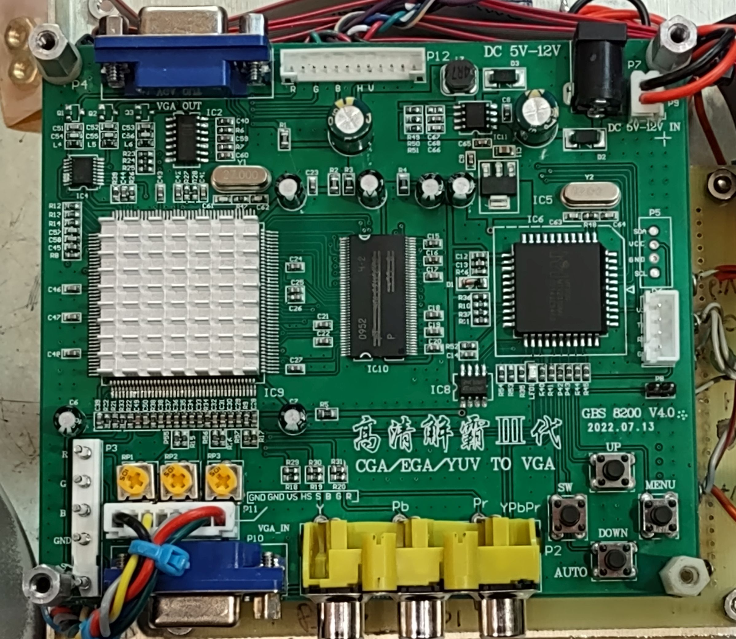
GBS-8200:

Figure 12:
The GBS-8200 video converter board.  This is "V4.0" of
the GBS-8200 which includes an on-board voltage regulator
allowing it to run from 5-12 volts.
Click on the image for a larger version.

There appear to be several versions of the GBS-8200 around - possibly from different manufacturers and some of these are designed to be operated from a 5 volt supply ONLY, but many have on-board voltage converters, allowing them to be operated from 5 to 12 volts:  The version that I have is the "V4.0" board with a "5-12 volt" input which eliminates the need for yet another voltage conversion step.  If you look carefully at the photo of the GBS-8200, the inductor for the buck converter is visible near the upper right-hand corner of the board, between the power connector the white video-out connector marked "P12" - but the silkscreened "DC 5V-12V" is also a big give-away!

This board, readily available via EvilBay and Amazon for well under US$40, is specifically designed to take a wide variety of RGB video formats - typically from 70s-90s video games and computers - and convert them to VGA format.  There are several connectors for video input seen along the bottom edge of the photo:  The three phono plugs for component video, an input on a VGA connector, and next to the VGA connector, two white headers for cable:  The unit that I purchased included a cable that plugs into the header between the VGA input and the three potentiometers.

At the top of the board, the VGA connector outputs the converted video - but there is also a white header next to it with these same signals.  As mentioned elsewhere, I simply soldered the six wires (R, G, B, H, V, and Ground) to the board, at this white header as I didn't happen to have another male HD-15 cable in my collection of parts.

This device can accept YUV and RGB inputs - and the latter can have either separate or composite sync inputs.  As the sync signals from the 4031 are non-standard, it's required that the sync processor described above produce a composite sync and the GBA-8200 be switched to the "RGBS" mode (using the "mode select" button) where the composite sync is fed into the "H-Sync" input and the "V-Sync" input is grounded.

The RGB inputs to the GBS-8200 come from the 4031, either as a single video source that is connected to all three inputs in the case of the "simple" (monochrome) version of the sync processor or from the RGB lines of the color version.  On board the GBA-8200 are three potentiometers visible in the photo above (near the lower-left corner) that are used to scale the input levels of the RGB signals to provide color tint/balance as desired.  In the lower-right corner can be seen the buttons used to configure the GBS-8200.

The "Splash" screen:

I've been asked how to get rid of the "splash screen" with Chinese characters when the unit is powered up.  This is from the GBS-8200 and (apparently) cannot be removed without flashing new firmware to it - which may be possible in theory.  The easiest way to suppress this screen would be to have a power-on delay of the LCD itself (or its back-light) that would wait until this screen had been displayed.  Such a device could be as simple as a 555 timer driving a relay with a 5-ish second delay.  Because this is a such a simple circuit - and a simple circuit board that can do this may be found on EvilBay and/or Amazon - I'll leave the implementation up to the reader.

External monitor:

The use of the GBS-8200 has an interesting implication:  It would be perfectly reasonable to use an external display with a VGA input (or VGA to HDMI converter) with the 4031.  This has the obvious advantage of being larger and the possibility of being placed conveniently when making adjustments where the 4031's itself may be too distant or awkwardly placed and small monitors like this are relatively inexpensive.  Additionally, it offers the possibility of being able to display to a larger group of people (e.g. teaching) and being digitized and recorded, as was done with the images at the bottom of this article.

Simply connecting a monitor to the VGA output of the GBS-8200 in parallel with the built-in LCD monitor would work - perhaps even as a short, permanent cord mounted to the rear (somewhere?) or hanging out of the 4031 should this be frequently required.  With a short (8", 20cm) "extension" cable permanently connected, any degradation caused by having an unterminated cable (when the external monitor was not connected) could likely be ignored and the rather low resolution of this display - as could be the slight diminution in brightness - when two monitors were connected at the same time (e.g. "double terminating").  Practically speaking, a buffer amplifier could be built to isolate the R, G, B and sync signals (using the simple emitter-follower circuit of Q1 see in Figure 8) to feed the external monitor.

Because there's no obvious place on the back panel to mount such a connector - and since I don't envision the frequent need for it - I did not so-equip my '4031.

Navigating the GBS-8200's menus

The four buttons used to configure the board are seen on the corner of the board at the top of the photo above.  Initially, the GBS-8200's menu system may be in Chinese, but the 4th menu allows the selection of either English or Chinese and it is changed to English with the following button-presses:

  • Menu - > UP -> Menu -> Menu 

At this point the text is now in English.

Other screens include:

  • "Display" - Which sets the output resolution:  A setting other than 640x480 is suggested.
  • "Geometry" - Which sets the position and sizes, along with how the blanking interval is to be treated.  Suggested initial settings are:
    • H position: 94
    • V position: 26
    • H size 56
    • V size: 66
    • Clamp st:  83
    • Clamp sp: 94
  • "Picture" - Which sets other display properties.  A setting of 50 is suggested for Brightness, Contrast and Saturation and a value of 05 is suggested for Sharpness.

The CLAA070MA0ACW display:

This is a 7" diagonal VGA screen of 4:3 aspect ratio and is available with a driver circuit board on EvilBay for around US$50.  Be sure that you get the version with the display controller board and not just the bare display panel, by itself. 

This unit is rated to operate from about 6 to 12 volts, and it comes with both an infrared remote and a small daughter board and interconnect cable that replicates the functions of the remote:  The remote is not required for this project as the daughter board and its pushbuttons will suffice.

Figure 13:
The driver board supplied with the CLAA070MA0A0ACW
LCD panel.  At the top is the VGA input while the TTL
to the panel is at the bottom, the back-light power connector
being in visible in the lower-right corner of the board.
Click on the image for a larger version.
The LCD panels themselves appear to be "pulls" from some consumer product (perhaps a portable DVD player?) as they have evidence of having been previously mounted, but the price is reasonable and their size is precisely that which may be used in lieu of the 4031's CRT, being a few millimeters larger than the window on the front of the 4031 in both axes making them a perfect fit by virtue of their being 4:3 aspect ratio:  It's possible that one could find a newer 16:9 that would fit horizontally in the available space, but it would likely leave a gap above and below the screen.

This unit will accept composite analog, HDMI and VGA, but it is VGA that we require, fed from the GBA-8200 via a short cable:  I constructed a very short (3", 7.5cm) cable, soldering one end directly to the GBA-8200 board itself (I could find only one 15 pin HD connector) just long enough to reach the VGA input connector of the display.  If desired, one could install a switch/distribution amplifier and provide a VGA connector to feed an external display - or likely get away with "double terminating" it as noted elsewhere.

This LCD came with a small board taped to the back of the display that is used to convert to a the flat ribbon cable supplied with the unit, used to connect to the display controller board via the "TTL OUT" connector:  This PC board should be glued to the back of the LCD panel with RTV or other rubberized glue (but not cyanoacrylate!) to mechanically secure it or else it is likely to work its way loose and tear the cable from the LCD panel.  When connecting to the "TTL OUT" connector on the main driver board, one must carefully lift up the locking lever (the black plastic piece that runs its width) from the back on the connector, slide in the cable, and push the lever back down.  The cable itself isn't marked as to which way is "up", but putting it in upside-down won't damage anything - but you'll see nothing on the screen:  Mark this cable when you determine its proper orientation.

There is also a short cable provided for powering the LCD panel's back light:  You won't likely see anything on the panel if this is not connected!

Figure 14: 
The original delaminating screen protector with EMI shield,
held in place with 10 screws and two brass angle pieces
around its perimeter.  This holds the front bezel in place.
Click on the image for a larger version.
Mounting the LCD panel:

The display is mounted "upside-down" (the wider portion of the metal border around the LCD panel being on top) to clear mechanical obstructions around the front panel of the 4031.  Fortunately, configuring for this display orientation can be accommodated via a menu on the display driver board as follows:

  • Select the "Function" menu
  • Go to "Mode"
  • Use the up/down buttons to select "SYS2"

The ONLY modification required of the 4031 to use the LCD display is mechanical.  Unlike the original CRT module - which was mounted in a large cavity behind the front panel - the LCD itself is mounted to the front panel of the 4031 while the other circuit boards (sync processor, GBA-8200,  CLAA070MA0ACW controller board) are mounted in the cavity formerly occupied by the CRT.

Figure 15:
The original screen protector (center) and copies, sitting atop
the laser cutter.  These were cut from 0.060" thick poly-
carbonate plastic.
Click on the image for a larger version.
Front screen protector: 

On the 4031s that I have, the CRT is protected by a plastic sheet containing embedded metal mesh for RFI/EMI shielding - which didn't actually seem to be grounded, anyway.

Unfortunately, over the years, this sheet tends to de-laminate and "bubble",  making viewing the screen rather difficult, so I duplicated a replacement using 0.060" polycarbonate using a laser cutter.  The use of polycarbonate over other types of clear plastic (like acrylic) is recommended due to its resiliency:  It can be bent nearly in half without breaking and is likely to stand the occasional impact from the connector of a cable or a bolt without cracking.  Acrylic, on the other hand - unless it is quite thick - would crack with such abuse.  For convenience, the dimensions of this screen protector are shown below.

While the original screens had EMI/RFI mesh embedded within them, these replacements will not.  The "need" for such shielding may be debated, but its worth noting that many similar pieces of equipment have no such shielding.  I did a bit of searching around for plastic windows with embedded mesh, but other than a few random surplus pieces here and there, a reliable source could not be found - but if you know if such a source, or even thin-wire widely-spaced mesh, please let me know.

Figure 16:
The dimensions of the screen protector - just in case
you might want to make your own!
Click on the image for a larger version.
One possible saving grace is the nature of the CRT versus the LCD:  A CRT has the potential (pun intended) to cause EMI owing to the fact that its surface is bombarded by an rapidly-changing electron beam that varies at MHz frequencies - and this can radiate a significant E-field.

The LCD, on the other hand, is a flat panel with low voltage and backed by a grounded metal plate, so the opportunity for it to radiate extraneous RF is arguably reduced.

Removing the front panel:

The front face of the 4031 comes off as a unit by removing the "Intensity" control knob, the two screws on either side that hold it into the unit's frame (the "second" screws from the top/bottom) and carefully unplugging three ribbon cables.  Inspection reveals that the screen protector is, itself, mounted to a bezel held in by several screws.

In my 4031, the original  the (de-laminated) front screen protector is extricated by removing the ten small screws around its perimeter (Figure 14)  and noting the way the pieces of brass angle that may be included are mounted - which allows it and front bezel to come out:  It looks to me like this screen protector may have been replaced in the past and it could be of slightly different construction than what was provided from the factory - but this is only a guess.

Figure 17:
After fully-tapping the 2.3mm screws, these aluminum angle
pieces with slots were attached to the aluminum bars seen
in Figure 14.  It is into these bars that the LCD panel, with
attached brackets, mount.
Click on the image for a larger version.

Removing the front screen protector will reveal two aluminum bars on either side - each with metal "finger stock" on the "inside" of the screen area - mounted to the front panel by countersunk screws hidden by the bezel that holds the screen cover.  Inspection will reveal that there are three holes along these bars that are not tapped all of the way through.  I removed these bars and purchased a 2.3mm tap and completed the threads so that I could insert 2.3mm x 6mm screws from the "other" (back) side.  It would have been about as easy to have drilled entirely new holes and tapped them for 4-40 screws (or your favorite Metric equivalent) and, in retrospect, I should have probably done so.

Using scrap pieces of aluminum, a pair of angle brackets were fashioned, held to the aluminum bars by the newly-tapped screws in those bars as seen in Figure 17.

To accommodate the momentary switch, I had to file away a portion of the bracket and bar on the left side ("behind" that in Figure 17 and this not visible) as well as countersink the back side of the plastic lens bezel so that it would accommodate the mounting hardware of the momentary switch and sit flush.

Into the brackets, slots were cut with a saw - also visible in Figure 17 - and it is into those that the angle pieces - now attached to the LCD - slide to allow adjustment of depth and very slight adjustment of axial rotation.  The LCD was located about 3/8" (10mm) behind the polycarbonate lens for clearance to protect the LCD panel itself should something be dropped on it - like a cable, RF connector or tool.
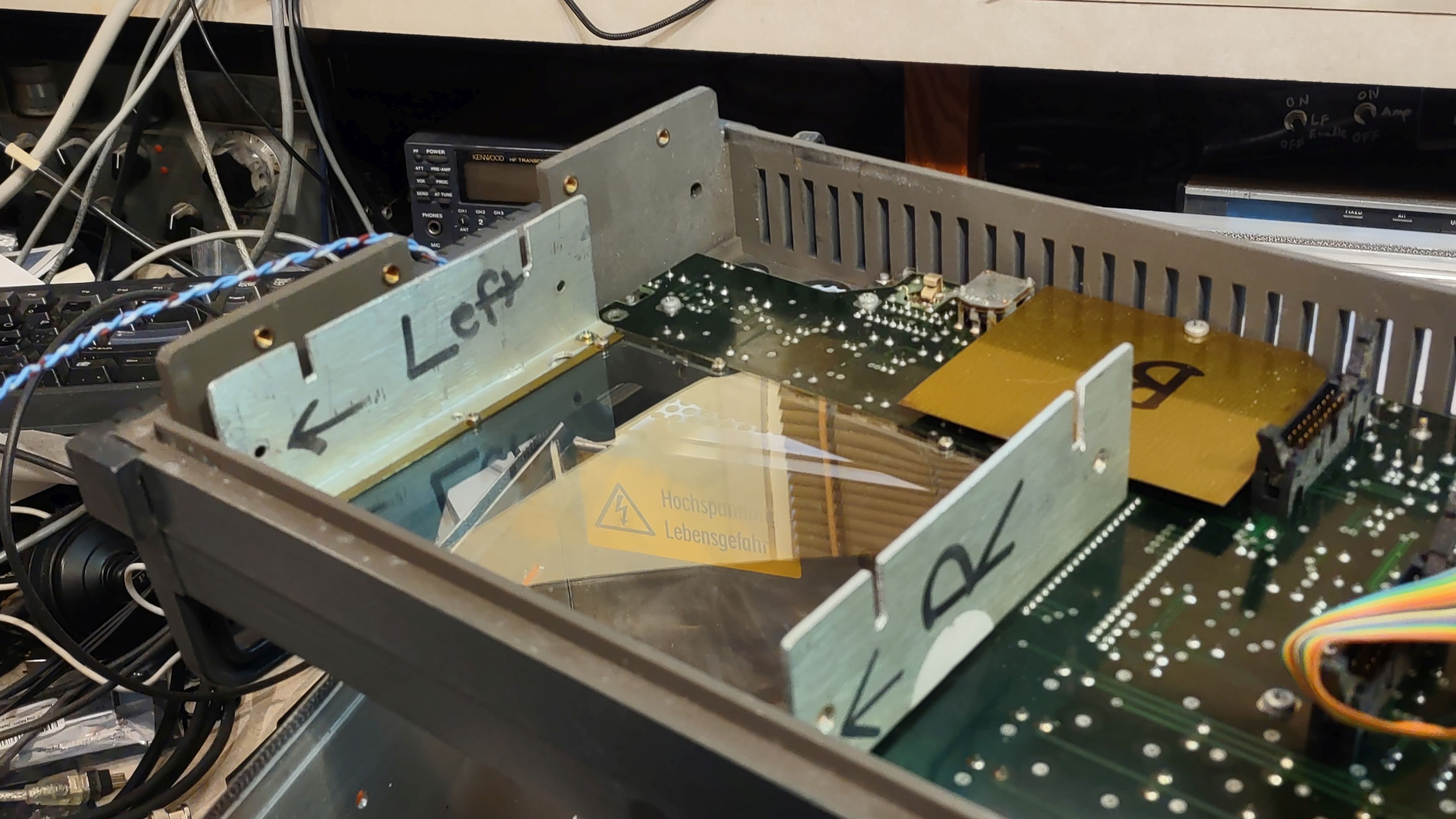
Figure 18:
The two brackets and new screen protector mounted in the
front panel assembly of the 4031.
Click on the image for a larger version.

As seen in the pictures, there is no obvious way to mount the display itself so a section of right-angle aluminum was cut and these were glued using "Shoe Goo" (a resilient rubber adhesive) to the back of the display itself, using the mounts fabricated to hold the display itself in position (described below) as a positioning guide:  It's likely that RTV (silicone) would have worked as well but I would not use an ineflexible adhesive like epoxy or cyanoacrylate ("Super Glue").

As this is done, it's very important to make sure that these brackets are installed correctly so that the display is both centered and square with the 4031's window:  I recommend actually mounting the display in place while the adhesive sets so that it perfectly fits the mechanical environment and there is no stress on the display itself as screws are tightened when it is mounted. When I did this, I put some "painters tape" on the front of the display and lightly marked it so that I could precisely set the horizontal and vertical position of the display with reference to the front bezel before the glue set.

Electrically connecting to the 4031:

Figure 19:
Two aluminum angle pieces with holes were glued to the back
of the LCD panel, now mounted in the front panel.
Click on the image for a larger version.
The connection of the original monitor to the 4031 is via an industry-standard 14 connection IDC ribbon cable/connector connected to the monitor and an exact duplicate was ordered from Digi-Key (P/N:  H1CXH-1436G-ND).  On this cable are the ground, power, sync and video connections as follows:

  • 1, 2:  +15 volts
  • 3-6:  Not connected
  • 7:  Vertical sync (positive-going pulse, TTL level, 50 Hz)
  • 8:  Ground
  • 9:  Horizontal sync (positive-going pulse, TTL level, 15.625 kHz)
  • 10:  Ground
  • 11:  Video  (positive-going, TTL level)
  • 12:  Ground
  • 13, 14:  Not connected

It's perhaps easiest to empirically determine these pins by stripping a small amount of insulation from the end of the wires and using a combination of volt/ohmmeter and oscilloscope to positively identify them, the ground pins being identifiable plugging in the other end of the cable and using continuity to the chassis with the unit powered down and then (carefully!) verifying them with the unit powered up, being very careful to avoid connecting the +15 volt wires to anything else.  Once identified, the wires that are marked as "not connected" were trimmed back slightly, the two +15 volt and three ground wires were (separately!) connected in parallel and the wires themselves colored using markers to aid in later identification.

Mounting the boards:

Figure 20:
The "stack-up" of the boards on the mounting sled.  Hidden
by the ribbon cable is the sync processor, above that is the
the GBS-8300 with its output VGA connector and above
that is the LCD controller with 4-button daughter board.
At the bottom, on the sled, may be seen the 7812
regulator used to drop the 15 volt supply to 12 volts.
Click on the image for a larger version.
A "sled" about 6" (155mm) wide and about 4.75" (120mm) tall - designed to be mounted to the left-hand wall (as viewed from the front panel) inside the enclosure.  This was constructed from a sheet of scrap aluminum and on it, the sync processor board, the GBS-8200 and the LCD controller were mounted using an assortment of stand-offs.  The different shapes and sizes of these boards complicated matters, so I had to be creative, resorting to mounting the LCD controller - and its daughter board (with pushbuttons and infrared receiver) to a piece of glass-epoxy PCB material that was, itself, held in place with stand-offs, seen in Figure 20 as the board on the vary top.

While I happen to have a bunch of stand-offs in my parts bins, I could have just as easily mounted the boards using long screws or "allthread" along with an assortment of nuts and washers.  These days, a more elegant custom mount could also be 3D-printed to hold these boards in place, although the metal "sled" and stand-offs offer a solid electrical connection to the chassis that may aid in RFI shielding and mitigation.

The only critical things in mounting are to provide access to the ICSP connector and R1 ("gray" adjust) on the sync processor board, the buttons on the GBS-8200, and the buttons on the daughter board on the LCD controller:  All of these should be accessible with just the top cover of the 4031 removed, without needing to disassemble anything else as depicted in Figure 21.

Figure 21:
Installed and powered- up, the stack-up of boards and
connected LCD panel.  All controls - and the ICSP
connector - are accessible simply by removing the top cover
of the 4031.
Click on the image for a larger version.
Into this "sled" were pressed self-retaining "PEM" nuts and it is mounted at four points in the same slots (using 8-32 screws) on the left side of the frame that were used to mount the original CRT monitor.

Powering the boards:

As noted above, the GBS-8200 is available in a version that may operate from 5-12 volts.  Similarly, the LCD panel's board can also accommodate up to 12 volts - but the 4031 supplies 15 volts.  During development, I ran both boards on the 4031's 15 volt supply directly with no issues, but I noted that 16 volt electrolytic capacitors were used on the inputs, so 15 volts would be pushing their maximum ratings.

Despite having no issues, I decided not to take a chance, so I added a 7812 voltage regulator, bolting it to the aluminum "sled" for heat-sinking (see Figure 20) and powering both the GBS-8200 and LCD panel from it.  As seen from the diagram above, the sync processor includes its own regulator (a 7805) and it may be powered from either 12 or 15 volts.

Overall results

Figure 22:
Under the shield of the "Monitor Control" board is R16, the
"width" adjustment that may be use to optimize video quality.
Click on the image for a larger version.

The results of all of this work look quite good as can be seen in the picture gallery below, but there are slight visual artifacts owing to the fact that the VGA conversion is from a device (the '4031) that does not have its pixel clock synchronized with the sampling clock of the GBS-8200 - or even the horizontal sync pulse.  The inevitable result is - if you look closely - that you may see some slight "glitching" on the leading or falling edge of vertical lines.

This effect can be reduce somewhat by adjusting the read-out pixel clock from the 4031's Monitor Control board.  Located on this board, under the shield, is potentiometer R16.  Nominally set to 11.0 MHz (as monitored at test point "Mp10") the frequency of this clock output may be reduced by turning this potentiometer slightly clockwise, reducing the effects of this aliasing somewhat by increasing the "width" of the display by making it output the line of video "slower".

If this adjustment is done, it should be done iteratively:  If it is set too low, the beginning of the line will start before the current line has finished drawing causing you to be able to see the left edge of the screen along the far right edge.  By adjusting the "Horizontal Width" on the GBS-8200, some of this overlap can be moved off the right edge of the screen so a balance between this and a low clock frequency must be found.  The approximate frequency set by R16 after this adjustment is between 7.75 and 8.0 MHz.

As mentioned earlier, trying to set a color horizontally across a scan line is not really practical:  The fact that, as we have seen, the pixel read-out rate is a free-running oscillator that is not synchronous with any of the the video sync pulses, so there is no "easy" way to synchronize a clock signal to set color attributes along the scan line from the video information alone.  To do so would require a sample of the pixel clock itself from the Monitor Control board!

In theory, it may be possible to tie the internal pixel clock to an already-existing clock signal on the Monitor Control board (e.g. the 8 MHz clock) to allow this and to reduce the "glitching" that is sometimes visible:  This modification is open to investigation.


Photo gallery

The following are screen captures obtained by first connecting a VGA-to-HDMI converter to the VGA output of the GBS-8200 board, and then connecting the HDMI output to a USB3 HDMI capture device meaning that the image is re-sampled several times in the process, accumulating artifacts. 


Figure 23:
The main "RX FM" screen.  The top portion is colored as light magenta to indicate an RX-FM screen while the center portion is colored in yellow.  The "soft" buttons on the bottom of the screen are given the attribute of a "gray" color.
Click on the image for a larger version.


Figure 24:
The TX FM screen, the top portion color-coded as light-cyan.
Click on the image for a larger version.


Figure 25:
The "duplex" screen, the top portion color-coded as light-green.
Click on the image for a larger version.

Figure 26:
The "oscilloscope" screen.  Because it is an "RX FM" screen, the top portion is colored with light-magenta, with the portion with the scope trace is colored light yellow.
Click on the image for a larger version.

Figure 27:
The analyzer display, color coded as light cyan as it's one of the "TX FM" modes.
Click on the image for a larger version.

Figure 28:
The Modulation Monitor "Zoom" screen, color coded as light magenta as it's one of the "RX FM" modes.
Click on the image for a larger version.


Video captured from the 4031:

Here is a short video,captured from the output of the GBS-8200, as the various screens are selected on the 4031:


At the end of the video, the monochrome modes (green, yellow, etc.) are selected in sequence.

Remember:  The video on the LCD mounted in the 4031 looks quite a bit better than is represented in the video - not only because it's a smaller screen, but the capturing of the video from the VGA output added yet another stage of analog digitization/degradation - plus there are artifacts from the YouTube video compression as well.

* * * * * * * * * * * * * * * * 

Why use a PIC?

One might ask, "Why did you do this with a PIC rather than an Arduino or a Raspberry Pi?"

First, I've been using the PIC Microcontrollers since the early 1990s, making good use of the CCS "PICC" compiler - (LINK) for much of this time:  This compiler is capable of producing fairly tight and compact code and I'm very familiar with it.  The PIC16F88 was chosen because it has the necessary hardware peripherals, it's easy to use, has plenty of RAM, program space and speed for this task, and is still available in DIP (and SMD) packages - a real plus in these days of "supply chain" issues.

The code running on the PIC uses interrupts and as such, it's possible that its same function could be done on a lower-end Arduino UNO as that processor sports similar hardware capabilities - but it's unlikely that this could be done using the typical Arduino IDE sketch environment, which does not, by default, lend itself to latency-critical interrupt processing.  You would have to get much closer to the "bare metal" and implement lower-level interrupts and some careful coding (possibly in mixed "C" and assembly) in order to have the code operate fast and consistently enough to do the pixel counting.

Another possibility is to use an ESP8266 or ESP32, but again one would need to get closer to the "bare metal" and optimize timing of the code to handle this sort of task - and you would still need to have the same sort of hardware (sync reprocessor, control of the RGB) signals.

Finally, a Raspberry Pi - if you can get one - would be overkill - and it would take MUCH longer for the RPi to boot up than the service monitor, which is up and running in under 15 seconds from power-up:  You would still need to interface the same signals (sync, video), but to 3.3 volt logic, and you would still need the same hardware (analog switches, etc.) to modify the video attributes - not to mention the time-critical code on a non-realtime operating system to do the pixel counting but this task could be done with additional hardware if needed.

Where can I get the code?

You may find the source code (for the CCS "PICC" compiler - I used version 5.018) and a compiled .HEX file for the PIC16F88 at the following links:

The .HEX code above is suitable for "burning" into a PIC16F88, and I use the PicKit3 programmer's ICSP (In Circuit Serial Programming) for this:  It's possible to reprogram the device in a powered-up 4031 - but because the code is written to detect when the ICSP is connected, it won't resume normal operation until the cable is disconnected.

As mentioned before, I have only one version of the 4031, so if your device has "different" screen signatures that result in pixel counts that don't match what's in the code, that screen will be rendered with white text.  Due to the complexity of the screen detection via pixel counting, making the recognition of the screen an automated process so that one could provide user-defined configurations would require a significant addition to the code - and likely the need for much more code space.

With the information provided it should be possible to apply this technique using other hardware platforms/microcontrollers - provided that one has either the speed to reliably count pixels at MHz rates and/or is able to get close enough to the "bare metal" of the processor to use on-chip peripherals to aid in the task.  In either case, close attention to the way the code operates - possibly a bit of optimization - will likely be required to pull off this task.

Final comments:

The most obvious change in the appearance of the 4031 after the modification - other than the colorized screen - is that of readability.  Clearly, the replacement of the degraded screen protector improved things considerably!

One advantage of the CRT - assuming that it is in good condition - is that it can be very bright, meaning that the LCD is at a slight disadvantage where high ambient light might be an issue:  In this case, one of the available "monochrome" modes may help.

The most obvious disadvantage of the LCD is that unlike the CRT, which has essentially a Lambertian emission profile from its surface (e.g. it radiates light hemispherically from the plane of the surface of the CRT), the LCD, by its very nature, has a comparatively reduced viewing angle.

When faced with viewing difficulties one would, in practice, simply relocate or reposition the 4031 so that it was more favorably oriented - and in some instances switching to one of the large "Zoom" screens may help when reading from a distance and/or awkward angle:  If you wish to do so, you could take advantage of the ability to use an external LCD monitor (small 7" units are fairly inexpensive) as described above.

Installing an LCD panel - with a blemish-free screen protector - and having "colorized" screens is a nice "refresh" of the 4031, particularly if you have been dealing with an ailing CRT for which there is no modern, drop-in equivalent.

* * * * * * * * * * *

This page stolen from ka7oei.blogspot.com


[END]


Wednesday, November 16, 2022

Using an inexpensive PT2399 music reverb/effects board as an audio delay (for repeater use)

Figure 1:
Inexpensive PT2399-based audio delay board
as found on the usual Internet sites.
Click on the image for a larger version.

In an earlier blog post (Fixing the CAT Systems DL-1000 and PT-1000 repeater audio delay boards - LINK) I discussed the modification of a PT2399-based audio delay line for use with the CAT-1000 repeater controller - and I also hinted that it would be possible to take an inexpensive, off-the-shelf PT2399-based audio effects (echo/reverb) board and convert it into just a delay board. 

While the uses of an echo-less delay for more mundane purposes may be apparent, it would be fair to ask why might one use an audio delay in an amateur radio repeater?  There are several possibilities:

  • The muting of DTMF ("Touch Tone") control signals.  Typically, it takes a few 10s of milliseconds to detect such signals and being able to delay the audio means that they can be muted "after" they are detected.
  • Reducing the probability of cutting off the beginning of incoming transmissions due to the slow response of a subaudible tone.  By passing COS-squelched audio through the delay - but gating it after the delay, one may still get the benefits of a tone squelch, but prevent the loss of the beginning of a transmission.  This is particularly important on cascaded, linked systems where it may take some time for the system to key up from end-to-end.
  • The suppression of squelch noise burst at the end of the transmission.  By knowing "before-hand" when an input signal goes away, one can mute the delayed audio such that the noise burst is eliminated.

Making good on the threat in the previous article, I reverse-engineered one of the PT2399-based boards available from Amazon and EvilBay and here, I present this modification, using one of these boards as a general-purpose audio delay.

The board:

Figure 2:
Schematic diagram of the audio delay board, with modification instructions.
This diagram is reverse-engineered from the board depicted in Figure 1.
Click on the image for a larger version.

The PT2399 boards found at the usual Internet sellers like EvilBay or Amazon are typically built exactly from the manufacturer's data sheet, and one of those found on the Internet for less than US$10 is depicted in Figure 1.  (Note that the chip may have another prefix in front of the number, such as "AD2399" or "CD2399")

The pictured board is surprisingly well-built, with plenty of bypassing of the voltage supply rails and a reasonable layout.  Despite the use of small, surface-mount resistors, it is fairly easy to modify, given a bit of care, and most of the components have visible silkscreen markings, making it easy to correlate the reverse-engineered circuit diagram (above) with the on-board components.

A few of the components do not have visible silkscreen markings (perhaps located under the components themselves?) and these are labeled in the circuit diagram and the board layout diagram (below in Figure 3) with letters such as "CA", "CB", "RA", etc.

Figure 3: 
Board layout showing component designations of the board in Figure 1.
Note that some of the components have no silkscreen markings and are labeled with letters
that have been arbitrarily identified as "CA", "CB", "RA", etc.
Click on the image for a larger version.

Removing the echo, making it delay-only

This circuit is the "bog standard" echo/reverb circuit from the app note - but it requires modification to be used as a simple audio delay as follows:

  • The output audio needs to be pulled from a different location (pin 14 rather than pin 15):
    • Remove R22, the 5.6k resistor in series with the output capacitor marked "CC".
    • A jumper needs to be placed between the junction of the (former) R22 and capacitor "CC" and pin 14 of the IC as depicted in Figure 4, below.
  • The feedback for the reverb need to be disabled and this involves the removal of capacitors C15 and C17.

Figure 4:
The modified PT2399 board, showing the jumper on pin 14
and the two flying resistors on the potentiometer, now used
for delay adjustment.  Note the deleted C15 and C17.
Click on the image for a larger version.

Figure 5, below, shows the schematic of the modified board with the changes described above.

At this point the board is converted to being a delay-only board, but with the amount of delay fixed at approximately 200 milliseconds with the value of R27  being 15k as seen in table 1, below.  This amount of delay is quite reasonable for use on a repeater to provide the aforementioned functions with no further modifications.

Optional delay adjustment:

By removing the need to be able to adjust the amount of echo/reverb, we have freed the 50k potentiometer, "RA", to be used as a delay adjustment as follows:

  • Remove R27, the 15k resistor, and replace this with a 47k resistor.  This is most easily done by using a 1/4 or 1/8 watt through-hole resistor and soldering one end directly to pin 6 and the other to ground, using the middle "G" pin along the edge of the board.
  • Remove R21 and using a 1/4 or 1/8 watt leaded 4.7k resistor, solder one end across where R21 went (to connect the wiper of potentiometer "RA") to pin 6 of the IC.
  • The 4.7k resistor (and parallel 47k resistor) sets the minimum resistance at about 4.3k while the maximum resistance is set by the parallel 47k resistor and the 50k potentiometer in series with the 4.7k resistor at about 25.3k.  These set the minimum and maximum delay attainable by adjustment of the potentiometer.

Of course, one may also use surface-mount resistors rather than through-hole components, using jumper wires rather than the flying leads of the components. 

Figure 5: 
Diagram of of the '2399 board after the modifications to be a "delay-only" circuit.
Click on the image for a larger version

This modification provides a delay that is adjustable from a bit more than 300 milliseconds to around 80 milliseconds, adjustable via the variable potentiometer. 

It's worth noting that if you do NOT  require a variable delay, using fixed resistors may offer better reliability than an inexpensive potentiometer of unknown quality - something to consider if the board is to be located on a remote repeater site.

If variable delay is not required, one would not use the 4.7k resistor at the junction of R21/"RA" - or use the potentiometer at all, and R27 would be replaced with a fixed resistor, the value chosen for the desired amount of delay as indicated in the following table:

Table 1: 
The amount of audio delay versus the resistance of R27.  Also shown is the internal clock frequency (in MHz) within the chip itself and the THD (distortion) on the audio caused by the delay chip.  As expected, longer delays imply lower bit rate and lower precision in the analog-digital-analog conversion which increases the distortion somewhat. 
This data is from the PT2399 data sheet.
Delay (ms) 
Resistance (R27)
Clock frequency (MHz)
Distortion (%)
342
27.6k
2.0
1.0
273
21.3k
2.5
0.8
228
17.2k
3.0
0.63
196
14.3k
3.5
0.53
171
12.1k
4.0
0.46
151
10.5k
4.5
0.41
136.6
9.2k
5.0
0.36
124.1
8.2k
5.5
0.33
113.7
7.2k
6.0
0.29
104.3
6.4k
6.5
0.27
97.1
5.8k
7.0
0.25
92.2
5.4k
7.5
0.25
86.3
4.9k
8.0
0.23
81.0
4.5k
8.5
0.22
75.9
4k
9.0
0.21

The chart above shows examples of resistance to attain certain delays, but standard resistor values may be used and the amount of delay interpolated between it and the values shown in the table.  

While not specified in the data sheet, the delay will vary with temperature to a slight degree as the onboard oscillator drifts, so it is recommended that the needed delay be chosen such that it will allow a slight variance while still providing the amount of delay for the needed task.

Comment: 

If this is to be powered from a 12 volt supply, it's suggested that one place a resistor in series with the "+" input to provide additional decoupling of the power supply.  The (possible) issue is that the 470uF input capacitor ("CA" on the diagram) will couple power supply noise/ripple into the ground of the audio delay board itself - and associated audio leads - potentially resulting in circulating currents (ground loop) which can induce noise.  Additionally, an added series resistance provides a modicum of additional protection against power supply related spikes.

The board itself draws less than 50 milliamps, and as long as at least 8 volts is present on the input of U4, the 5 volt regulator, everything will be fine.  A 1/4-watt 47 ohm resistor (any value from 33 to 62 ohms will work) will do nicely. 

* * * * * * *

Addendum:  Adding audio switching

Since the original publication of this post there have been several questions as to how to "switch" audio to the delay board.  In many cases, this will not be required as the device being used (say, a repeater controller) may already have an audio gate - but in the event that you really do need to switch audio on/off - or switch it between "A" and "B", refer to Figure 6, below.

Figure 6:
Examples of using the 4066 quad audio gate for audio gating and switching.
Both an "on/off" gate and "A/B" switch - plus using a 4066 to generate an inverted logic signals - is depicted.
Click on the image for a larger version.

How it works:

For the audio switching we will use the 4066 quad analog switch.  In this example, we are using the CD4066 - the "old school" 4000-series CMOS which can operate between 3 and 15 volts.  The "newer" "HC" logic versions may also be used, but their maximum voltage is either 5 or 6 volts, depending on the specific part used. 

The "On/Off" gate:

Let's take the On/Off gate as the first example.  Note that the input/output ports - which are interchangeable (e.g. the switch is bidirectional so it could even be used with bidirectional signals) - are biased with R201 and R202 which sets the resting DC voltage at about 1/2 the supply voltage from the circuit marked "V+/2 Source".  Capacitors are used on these lines to block this DC bias voltage from appearing on the In/Out lines and disrupting the bias.  If you are switching audio lines with DC already on them, be sure to consider the polarity of the blocking capacitors in the event that this "external" audio source's voltage is higher than V+/2.

The reason for adding a bias voltage to the In/Out audio is to prevent the audio swing from causing the protection diodes found on this (and almost all other) chips from conducting if it exceeds either V+ or goes "below" ground:  Doing so would likely cause distortion of the audio on the positive and/or negative peaks.

Note that the bias is applied to both the input and output.  This is done to prevent an audio "click" or "pop" that would occur when the switch was closed:  If the DC voltages weren't exactly equal on the in/out lines when the switch was open, closing (turning on) the switch would cause a sudden change in the form of a click.

The "A/B" gate:

If you wish to switch two different audio signals from the same logic signal by turning one or the other on, this circuit is a replication of the "On/Off" gate - but it uses another 4066 gate as a logic inverter.  When the "A" switch is on, U1d - the middle switch - is also turned on, shorting R303 to ground which turns of the "B" switch.  When the "A" switch is turned off by setting its logic level to low, U1d is now turned off but the control line for the "B" switch is pulled high by R303, turning it on.

While the example shows two separate switches, one could connect them together, tying one of the in/out lines of each switch together as the common in/out port if you wished to use it to select source "A" or source "B".  If you do this, you could probably eliminate one of the blocking capacitors - but there's little harm if leaving it there if you are unsure as to what to do.

The "Low Voltage Logic to High Voltage Logic" converter:

All digital ICs have threshold voltages for their logic inputs - and the 4066 is no exception.  If you operate the 4066 gates from 12 volts, you will need "about" 12 volts on the "control" pin to properly "turn on" the audio gate:  Applying, say, 5 volts to it as a "high" signal probably won't work so the voltage of this control signal must match the supply voltage of the switch chip.

This is a very simple one-transistor logic level converter.  In the event that you have, say, a repeater controller that has 3.3 volt logic, but you choose to power the 4066 audio switches from 12 volts, you can use this to derive the 12 volt logic level needed to properly switch.  One downside of this circuit is that it will "invert" the logic signal:  Input a "1" (high voltage) and you get a "0" (low voltage) on the output.

Depending on the audio control signal from your controller, it may already be a "low active" type - or it may be programmable.  In the event that you need to do a high voltage logic level and  that it NOT be inverted you can put two of these one-transistor circuits in series.  If you are already needing to switch between audio "A" and "B", you wouldn't need to do this as you could simply swap "A" and "B" if you end up with an "inverted" control signal.

Selection of power supply voltage:

As mentioned, the CD4066 may operate from anywhere from 3 to 15 volts:  12 volts is sometimes convenient as that may be the unregulated input voltage of the main power supply - but what voltage is appropriate?

The supply voltage should be equal to or higher than the peak-to-peak audio signal - something that can only be measured accurately with an oscilloscope.  For example, if you have a repeater and the peak audio voltage from the audio line when the receiver is running open squelch with no signal is 8 volts, you should NOT power the 4066 audio gate from 5 volts - but 10 or more volts would certainly provide adequate headroom.  If your audio level peak-to-peak voltage exceeds the power supply voltage, the audio will be clipped by the 4066's protection diodes and cause audio distortion.

If, in the above example, the peak voltage from the squelch noise was only 3.5 volts peak-to-peak, you could operate the 4066 from a 5 volt supply, saving you the need for logic level conversion and alsopermitting the use of the "74HC4066" instead.

Consideration of impedance:

These switches are intended for "high" load impedance (typically 10k or more) audio input rather than for audio switching where the LOAD impedance is low - such as a speaker.  The reason for this has to do with the resistance of the 4066 gates (which could be 10s or 100s of ohms) and, to a lesser extent, the value of the blocking capacitors  Fortunately, the input impedance of most sources on which this would be used (audio amplifier, repeater controller) are typically quite high.

* * * * * * *


This page stolen from ka7oei.blogspot.com

[END]


Sunday, October 30, 2022

An ultrasonic superheterodyne receive converter (e.g. "Bat Listener")

In the mid 90s I decided to throw together what I called a "Bat Listener" - a simple receiver used to convert ultrasonic sound down to the audible range.

Figure 1:
The exterior of the ultrasonic receiver, complete with fancy
labeling!
Click on the image for a larger version.

Two types of circuits:

There are two common ways to convert a higher (ultrasonic) signal to the audible range, whether this is done using analog or DSP (Digital Signal Processing) techniques.

Frequency division

There are several ways to do this, the simplest being the "divider" type which digitally converts ultrasonic frequencies to audible by integer division of the input to a lower frequency.

The problem with this simple approach is that it does not preserve the amplitude (loudness) of the original sound since it must take the input signal, amplify/convert it to a series of logic-level pulses - which loses any amplitude reference - and do a brute-force digital division.  Additionally, if there are multiple signals present, for the most part only the strongest one will be converted down.

Clearly, one cannot "tune" this type of circuit:  A signal at 40 kHz will always be divided down by a fixed integer amount,  Let's say that the circuit digitally divides by 32:  That 40 kHz signal will be at 1.25 kHz.

Additionally, the direct "A-B" frequency differences between ultrasonic signals is lost, instead being "(A-B)/N" where "N" is the number of divisions.  In other words, the relative frequency differences between signals is not preserved.

Heterodyne conversion

The other way to do this is to convert the frequency.  In this technique, two signals - the ultrasonic to be converted - and another generated by the device (the "local" oscillator) are mixed together.  The result is an arithmetic shift in frequency.

The biggest advantages of this method are the fact that that not only are the differences in frequency preserved (e.g. two tones 1 kHz apart at ultrasonic will appear as two tones 1 kHz apart at audio) but the relative amplitudes (loudnesses) of the received signals are preserved as well.

Frequency conversion:

I chose to build a heterodyning receiver to convert the input frequency to a lower one.  This can preserve the amplitude and frequency relationships  - plus it is fully tunable, allowing one to choose the frequency range to convert to audible sounds - and since it is a simple conversion, multiple signals present will also be preserved.

When it comes to frequency conversion, there are two ways:  The simplest - direct conversion - would involve mixing a variable oscillator with the incoming signal and filtering/amplifying the resulting audio.  This has the advantage of being the easiest, and it is the method described in this article:

     April, 2006 QST article, A Home-made Ultrasonic Power Line Arc Detector - link)

A similar device - the MFJ-5008 - was made by MFJ Enterprises, but as this company is no longer doing business, it is found only on the used market.

While I could have easily built something like this a decade before the above article was published, as I'm sometimes wont to do I decided to make it a bit more complicated, constructing a superheterodyne converter.

While a direct-conversion receive simply mixes an oscillator with the desired signal to cause a frequency conversion, a superheterodyne receiver operates like a conventional AM or FM radio:  The desired signal is first converted to an IF (Intermediate Frequency) - and this IF is then converted to audio.  The advantage of the superheterodyne scheme is that filtering may be applied at the IF to limit the receive bandwidth - and since the IF is fixed, its width remains constant over the tuning range, just like that in a conventional radio/receiver.

Circuit description

Figure 2:
Schematic diagram of the superheterodyne ultrasonic receiver.
See text for a circuit description.
Click on image for a larger version.
 

As noted above, this circuit is more complicated than it needs to be, so make of it what you will!

VCO:

The heart of the unit is U1, the VCO (Voltage Controlled Oscillator) which uses the venerable CD4046 PLL chip.  Often used for frequency synthesis, we are using (only) the oscillator portion, which provides a linearly-tuned and fairly stable frequency source, adjusted by the voltage applied via R101 (and scaling resistor R102).  The values were chosen to provide an approximate frequency range of 125 to 185 kHz (more on this later) to allow tuning of audio signals from (ostensibly) 0 to about 60 kHz.  The actual tuning range is closer to 115-190 kHz as a bit of extra margin for the frequency range.

The only critical component here is C101 which should be a frequency-stable capacitor.  I used a polystyrene capacitor, but an NP0 (a.k.a. C0G) or silver-mica could be used, instead.  When I reverse-engineered this device, I noted that the marked capacitance value was unreadable, but back-of-the-envelope calculates indicate that a value of "about 150pf" should be in the ballpark.

R103, connected to the "R1" pin of U1, sets the approximate center frequency range while R104, connected to the "R2" pin - sets the lowest frequency - which important, since we want to constrain the tuning to 125-185 kHz.  Additionally, the low end of the tuning range was further refined by R102 on the "ground" side of the tuning potentiometer, which sets the minimum voltage that may be applied to the "VCOIN" pin.

The VCO output, a square wave, is buffered by U2, a hex inverter, and several sections are used to provide both a VCO signal and its inverted version to drive the mixer.

While the 4000 series CMOS chips throughout this receiver will happily run from 3-15 volts, they are operated from a regulated 5 volt supply - mainly to improve frequency stability and to provide a nice, stable voltage for a few other low-level circuits and to provide isolation from the main battery supply which will vary a bit, particularly at higher receive volumes:  This variance, if it gets back into some earlier stages, could cause instability of the receiver in the form of "motorboating" (low-frequency oscillation or pulsing) or some other type of feedback.

BFO:

Another circuit is the BFO (Beat Frequency Oscillator) which is used to convert the IF signal back down to audio - both being processes that we'll discuss shortly.  This uses an inexpensive 500 kHz ceramic resonator to form an oscillator using one of the sections of U2C, the signal being buffered by U2B.  This signal is divided-by-two using U3A, one half of a 4013 dual flip-flop - and then divided by two again using U3B, yielding a stable 125 kHz signal.  As with the VCO, two phases of this signal (normal and inverse) are available, this time using the "Q" and "!Q" outputs of the 4013.

Input signal path:

J1, a disconnect-type 3.5mm stereo jack is wired so that an internally-mounted electret "capsule" microphone is connected by default.  This microphone element (M301) is of the "2 wire" type or electret microphone in which a bias voltage is applied to the same pin from which audio is drawn - this voltage being applied via R301 from the 5 volt regulated supply.  The specific make/model of this electret element is unknown as it was selected from a small collection to find the best performer at ultrasonic.

Using a MEMs microphone

Since this article was first written, I replaced the electret with a more modern MEMs microphone as described in Another article:  Improving my ultrasonic sniffer for finding power line arcing by using MEMs microphones - link.  These types of microphones are capable of detecting from low audio frequency (a few 10s of Hz) and much higher - often through 100 kHz.

The schematic in Figure 2 now shows how an ANALOG MEMs microphone (see the link above for more information) may be integrated into the unit.  As these microphones are not tolerant of 5 volts, I used some "normal" (not "high brightness") GaAsFET Green LEDs:  D401 limits the voltage to 1.8-2.0 volts on the microphone's power supply while D402 prevents "glitches" from damaging the MEMS device that might get through via coupling capacitor C402 when an external microphone is connected/disconnected.  When everything was done, there was a very dramatic improvement in sensitivity above 15 kHz and several switching supplies near the workbench - which I couldn't hear before - suddenly became very audible.

Microphone amp and filtering

The signal from the microphone is applied to U4A which is wired as a unity-gain buffer.  For this, an LM833 is used, an inexpensive, low-noise dual op amp:  An LM358 or many other types may be used here as well - just make sure that it is is fairly low noise:  I'd avoid the use of the LM1458 here as it is quite noisy by comparison!

Section U4B amplifies the signal voltage by 10 (20 dB of power gain) and this signal is applied via R305 to a simple L/C high-pass filter consisting of C303, C304, L301 and L302 the latter two components being inexpensive 18 milliHenry inductors.  Certainly, an R/C-based high-pass filter could have been constructed using U4B, but I chose not to do that for some reason.

Figure 3:
Inside the ultrasonic receiver, constructed on
prototype board and having been modified
several times over the years, prior to the
installation of the MEMS microphone.
Click on the image for a larger version.

In simulation, the C303/C304/L301/L302 filter has a -3dB roll-off of about  23 kHz, it's down by 10dB at about 19.5 kHz, by 20dB at about 16 kHz and by 40 dB at 9 kHz and with the values shown, it's flat to within 1 dB between about 24 and 100 kHz.

The output of the filter is amplified by U5B - and then even more by U5A (which has a bit of roll-off from C307) to yield a whole lot of gain.  It's very possible that I over-did the gain here, but unless the signal source is quite close, there is no clipping observed on the output of U5A.

Its worth noting that a mid-supply voltage is created using R309/R310 to provide a "virtual ground" for the op amps and to maintain stability, it is heavily filtered by C306 and C302, each located near the respective op amp shown on the diagram.

Mixer and band-pass filter:

It is this next section that may seem unfamiliar to some - the use of a CMOS analog switch as a signal mixer.  For this, a CD4066 is used which consists of four separate analog switches.  The filtered and amplified ultrasonic input signal from U5A via C308 is applied to pins 2 and 10 of U6A/U6D.  When the respective signals on the control pins "VCO_A" and "VCO_B" go high, the switches are activated, and because VCO_A and VCO_B are inverts of each other, each of these switches is closed in turn.  The result of this is that the inputted signal is chopped up at the rate of the 125-185 kHz VCO and this produces two mixing products.  

For example, let's assume that there is a 40 kHz signal is present on the input that we wish to hear.  If the VCO is tuned 40 kHz above the 125 kHz IF (again, more on that momentarily) - to a frequency of 165 kHz - the switching action of U6A and U6D produces both the sum (165 + 40 = 205 kHz) and the difference (165 - 40 = 125 kHz).

T301 is a filter/transformer that passes only the 125 kHz signal - the difference signal in this case.  This transformer consists of two separate windings, each resonated using its internal capacitors and the externally-added 820 pF capacitors on each winding (e.g. C309/C310) to "pad" it down to 125 kHz.  This forms a fairly wide (8-10 kHz) filter that rejects signals outside the immediate vicinity of its 125 kHz frequency.  Because this filtering is at a fixed frequency, it does not vary with input tuning which means that its bandwidth is constant over frequency.

Of all of the components in this device, this transformer is unique:  It was originally a 262.5 kHz IF transformer from a 1970s/1980s Philco (Ford) AM-only car radio.  While I could have certainly used the original 262.5 kHz frequency - or even 250 kHz, when I built this I decided to pad it down to 125 kHz using C309/C310  - a frequency that is conveniently 1/4th of the 500 kHz resonator.

It's been so long since I built this, I don't recall why I didn't simply divide the 500 kHz by two and readjust that transformer to 250 kHz.  Practically speaking, I could have also up-converted to 455 kHz and used either transformers or ceramic filters from a modern AM radio as 455 kHz ceramic resonators were certainly available at the time - but I didn't do that.

Each half of T301 has a center tap and to this, a bias voltage is applied via R315 to assure that the voltage on these switches was in the middle of the supply range, away from the protection diodes on the 4066's I/O pins, which could cause clipping/distortion should they be allowed to conduct if the signal voltage got too near the ground or supply rails.  To prevent coupling between the two halves of the transformer via the center tap, R314/C311 was added, the resistor adding isolation with the capacitor bypassing the remainder of the signal.  Practically speaking, being able to adjust the bias voltage was unnecessary as a simple resistive voltage divider to set the bias at 2.5 volts (1/2 the supply voltage) would have been just fine.

On the "other" side of the transformer is the other half of U6 (e.g. U6B/U6C) - this time, clocked from the fixed 125 kHz oscillator.  From this, the signal - previously converted up to 125 kHz is now converted back down to audio.

Post-mixer amp/LPF:

The output of the down-converting mixer is applied to U7B via R316, a 1k resistor and a 0.001uF capacitor, both of which form a simple R/C low-pass filter to attenuate any high-frequency leakage signals from the mixer.  Because the mixing process itself is a bit lossy (about 25% efficient) as is transformer/filter T301, U7B boosts the signal by a factor of 10 (20dB) and then applies it to U7A, which is configured as a variable gain amplifier section.  The output of this is then boosted again by U8, an LM386 which is capable of driving headphones or even a small speaker.

A few comments about the design:

Originally, the circuit lacked U7 at all, but it was added when the gain of U8 (the audio amplifier), by itself, was found to be inadequate.  Since U7 was "patched" into place, this explains the odd gain distribution:  If I were rebuilding this from scratch, I'd certainly not need two post-mixer amplifier sections and I could have likely eliminated one full dual op-amp package.  As it is, I may add a "high/low" gain switch somewhere around U5 to allow reduction of the gain somewhat when in the presence of possibly-high ultrasonic signal levels to prevent clipping prior to the band-pass filter which would surely degrade overall performance.

If I were to build this again I would likely use a 455 kHz IF, instead as noted.  While not as plentiful, 455 kHz ceramic resonators are available to use for the BFO as are either transformer or ceramic-based band-pass filters.  I would also likely reconfigure U4B or U5 to perform the high-pass filter function rather than using harder-to-find inductors.

Again, I built this unit in the mid 1990s and have since lost my original notes, but I do recall that I modified it a few times since, simply tacking changes onto the old circuit rather than completely revising it.

Use as a longwave receiver:

While primarily intended to "hear" ultrasonic sounds such as those produced by bats, insects, leaking pipes, arcing power lines, etc., it is just a longwave radio receiver connected to a microphone:  If one connects a few 10s of feet/meters of wire to to J1 - and provides an Earth/ground reference to its shield connection - one can easily tune in the high-power transmitters used for submarine communications (around 20-30 kHz) plus the WWVB time signal at 60 kHz.  This must, of course, be done away from man-made noise sources such as power lines.

Alternatively, I have used a loop of about 1 foot (25cm) diameter of a dozen or so turns of wire along with a 10uF capacitor in series (to optionally block DC from R301) and been able to hear such signals - even in suburbia - but with this arrangement you'll also likely hear plenty of similar signals from the myriad switching supplies that likely inhabit your house as well!

Final comments:

The reader should be under no illusion that this is an optimized circuit or that I would do it this way again:  It was assembled fairly quickly to suit a need and to test a few random ideas, just to see if they would work.  Will I rebuild it at some point?  I don't know - it works as it should, so I don't plan to re-make something that is currently fit for purpose.

While I've heard very few bats with this - probably due to the deficiencies of the electret microphone at ultrasonic frequencies (which explains the future switch to MEMS-type microphones) - I've used it to find powerline noise (arcs are noisy at ultrasonic) and to test longwave receive antennas.

This page stolen from ka7oei.blogspot.com

[End]


Tuesday, September 27, 2022

Using an ATX computer power supply to run KiwiSDRs - and as a general purpose 5 and 12 volt supply

At the Northern Utah WebSDR (link) we run a number of KiwiSDR receivers.  These receivers, which are inherently broadband (10 kHz to 30 MHz) allow a limited number of users to tune across the bands, allowing reception on frequencies that are not covered by the WebSDR servers.

At present there are six of these receivers on site:  Three are connected to the TCI-530 Omnidirectional antenna (covering 630-10 meters - 2200 meters is included via a separate E-field whip), two are on the east-pointing log-periodic beam antenna (which overs 40-10 meters) and the newest is connected to the northwest-pointing log-periodic beam antenna (which covers 30-10 meters).

Figure 1:
Power supply in a PC case!
The PC case housing the power supply was repurposed -
because, why not?
Click for larger version
The power requirements of a KiwiSDR are modest, being on the order of 600-800 mA, but the start-up current can briefly exceed 1.25 amps.  Additionally, they do not start up reliably if the voltage "ramps up" rather slowly - a problem often exacerbated by the fact that the extra current that they draw upon power-up can cause a power supply to "brown out".

Up to this point we had been running 5 KiwiSDRs:  Three of them were powered by a pair of 5 volt, 3 amp linear power supplies that are "dioded-ANDed" together to form a 6 amp power supply and the other two KiwiSDRs were powered from a heavily-filtered 5-volt, 3 amp switching power supply.

In recent months, the dual 3 amp linear supply had become problematic, not being able to handle the load of the three KiwiSDRs, so we had to power down KiwiSDR #3.  With the recent installation of the northwest-pointing log periodic antenna, we were also looking toward installing another KiwiSDR for that antenna and we were clearly out of power supply capacity.

Using an ATX supply as a general-purpose power supply - it's not just the green wire!

If you look around on the Web, you'll see suggestions that you just "ground the green wire" to turn on an ATX supply, at which point you may use it as a general-purpose supply.  While grounding the green wire does turn it on, it's not as simple as that - particularly if you leave the power supply unattended.

For example, what if there is a brief short on the output while you are connecting things, or what if the power browns out (or turns off) for just the "wrong" amount of time.  These sorts of things do happen, and can "trip out" the power supply and it may never restart on its own.

With the site being remote, we couldn't afford for this to happen - so you'll see, below, how we remedied this.

Putting together another power supply:

With six KiwiSDRs, the power supply requirements were thus:

  • 5 amps continuous, making the assumption that a KiwiSDR's average current consumption would be about 830 mA - a number with generous overhead.
  • 9 amps on start-up, presuming that each KiwiSDR would briefly consume 1.5 amps upon power-up, again a value with a bit of overhead.
  • The power supply must not exhibit a "slow" ramp-up voltage as the KiwiSDRs did not "like" that.

In looking around for a power supply on which to base the design, the obvious choice was an computer-type ATX power supply.  Fortunately, I have on-hand a large number of 240 watt ATX supplies with active power factor correction which are more than capable of supplying the current demands, being rated for up to 22 amps load on the 5 volt supply - more than enough headroom as I would be needing less than half of that, at least with the currently-planned usage.

Circuit description:

Refer to the schematic in Figure 2 for components in the description.

Added filtering:

While these power supplies were already known to be adequately RF-clean (important for a receive site!) from their wide use for the WebSDR servers because we would be conducting the DC outputs outside the box - and to receivers - I felt it important that additional filtering be added.  Having scrapped a number of PC power supplies in the past, I rummaged around in my box of random toroids and found two that had probably come from old PC power supplies, wound with heavy wire consisting of 4 or 5 strands in parallel.  These inductors measured in the area 10s of microHenries, enough for HF filtering when used with additional outboard capacitance.

These filter networks were constructed using old-fashioned phenolic terminal lug strips.  These consist of a row of lugs to which components are soldered - typically with one or two of the lugs used for mounting, and also "grounding".  Rather than mount these lugs using a drill and screw, they were soldered to the steel case itself - something easily done by first sanding a "bare" spot on the case to remove any paint or oxide and then using an acid-core flux - cleaning it up afterwards, of course!

The heavier components (inductors, capacitors) were mechanically secured using RTV (silicone) adhesive to keep them from moving around - and to prevent the possibility of the inductor's wire from touching the case and chafing.

Looking at the schematic you may note that  C202, C302, C501, C502 and C503 are connected to a "different" ground than everything else.  While - at least for this power supply - the "Common" (black) wire is internally connected to the case, it's initially assumed that this lead - which comes from the power supply - may be a bit "noisy" in terms of RF energy, so they are RF bypassed to the case of the power supply.  This may have been an unneeded precaution, but it was done nonetheless.

Connectorizing and wiring the power supply:

The ATX power connector was extracted from a defunct PC motherboard to allow the power supply itself to be replaced in the future if needed.  On this connector, all of the pins corresponding with the 5 volt (red wires), 12 volt (yellow wires) and ground (black wires) were bonded together to form three individual busses and heavy (12 AWG) wires were attached to each:  This was done to put as many of the wires emerging from the power supply in parallel with each other to minimize resistive losses. 

The green wire (the "power" switch) and purple wire (the 5 volt "standby") were brought out separately as they would be used as well - and the remainder of the pins (3.3 volt, -12 volt, -5 volt, "power good", etc.) were flooded with "hot melt" glue to prevent anything from touching anything else that it shouldn't.

The 5 volt supply was split two ways - each going to its own L/C filter network (L501, L502, C502, C503, C504, C505) as shown in the schematic, this being done to reduce the total current through the inductor - both to minimize resistive losses, but also to reduce the magnetic flux in each inductor, something that could reduce its effective inductance.

Although I don't have immediate plans to use the 12 volt supply, a similar filter (L503, C506, C507) was constructed for the 12 volt supply lead.  On the output side of the 12 volt filter, a 3 amp self-resetting thermal fuse (F501) was installed to help limit the current should a fault occur. 

About the self-resetting fuses:

 These fuses - which physically look like capacitors - operate by having a very low resistance when "cold".  When excess current flows, they start to get warm - and if too much current flows, they get quite hot (somewhere above 200F, 100C) and their internal resistance skyrockets, dropping the current to a fraction of its original value:  It's this current flow and their heat that keeps the resistance high.

It's worth noting that these fuses don't "disconnect" the load - they just reduce the current considerably to protect whatever it is connected to it.  Since, when "blown", they are hot, they must be mounted "in the clear" away from nearby objects that could be damaged by the heat - and also to prevent lowering of their trip current by trapping heat or being warmed by another component - such as another such fuse.  

It should be noted that if the outputs - either 5 or 12 volts - are "hard shorted", the thermal fuse may not react quickly enough prevent the power supply from detecting an overcurrent condition and shutting down.  As an output short is not expected to be a "normal" occurrence, this behavior is acceptable - but it will require that the power supply be restarted to recover from shutdown, as described below.

In the case of the KiwiSDRs, they are connected with fairly long leads (about 6 feet, 2 meters) and often have enough internal resistance to reduce the current below the power supply's overcurrent limit and rather than allowing the full current of the power supply (which could be more than 20 amps) to flow through and burn up this cable, the fuse will trip as it should, protecting the circuit.  To "reset" the fuse, the current must be removed completely for long enough for the device to cool - something that is done with the 5 volt supplies as we'll see, below.

The controller:

As mentioned earlier, if you look on the web, you'll see other power supply projects that use an ATX power supply as a benchtop power source and most of those suggest that one simply connect the green (power on) wire to ground to turn it on - but this isn't the whole story.  In testing the power supply, I noticed two conditions in which doing this wouldn't be enough:

  • Shorting a power supply output.  If the output of a good-quality ATX power supply is shorted, it will immediately shut down - and stay that way until the mains power is removed (for a minute or so) or the power supply is "shut off" by un-grounding the green wire for a few seconds before reconnecting to "restart" the power supply.
  • Erratic mains power interruption.  It was also observed that if the mains power was removed for just the right amount of time, the power supply would also shut down and would not restart on its own.  It took the same efforts as recovering from an output short to restart the power supply.

Since this power supply would be at the WebSDR site - an unmanned location in rural, northern Utah - it would require additional circuitry to make this power supply usable.

Fortunately, an ATX power supply has a second built-in power supply that is independent of the main one - the "standby" power supply.  This is a low-power 5 volt supply that is unaffected by what happens to the main supply (e.g. not controlled by the power switch and not affected if it "trips off") and can be used to power a simple microcontroller-based board that can monitor and sequence the start-up of the main power supply.  For this task I chose the PIC16F688, a 14 pin microcontroller with A/D conversion capability and a built-in clock oscillator.

As seen in the schematic, the "5 volt standby" is dioded-ORed (D601, D602) with the main power supply (12 volts) so that it always gets power - from either the 5 volt standby, or from the 12 volt output - when mains is applied.  R603 and capacitor C602 provide a degree of protection to the voltage regulator should some sort of "glitch" appear on the 12 volt supply - possibly due to the 5 volt load being abruptly disconnected (or connected) as the 5 and 12 volt supplies are "co-regulated" in the sense that it's really only the 5 volt output that is being regulated well - the 12 volt power supply's output is pretty much a fixed ratio to the 5 volt and doesn't really have much in terms of separate regulation.

It should be noted that when operating from the standby +5 volt power source, the voltage from U2 (the 5 volt regulator) is on the order of 3 volts or so (drop through D602 and U2) but this is comfortably above the "brownout" threshold of the PIC, which is around 2.5 volts, so there isn't really a worry that the low-voltage brownout detector will trigger erroneously and prevent start-up.  If it had, I would have simply moved the cathode side of D602 to the +5V side of U2.

Figure 3: 
Inside the case!
Top right:  12 volt supply filtering and thermal fuse
Upper-middle:  Dual 5 volt filtering
Lower middle:  Controller board with FET switches
and thermal fusing.
The ATX power supply is in the lower-left corner.
Click on the image for a larger version.
Because the PIC microcontroller can monitor the 12 volt supply (via R601/R602) it "knows" when the main ATX supply is turned off.  Through the use of an NPN transistor (Q401) - the collector of which can be used to "ground" the green "power on" line, the controller can turn the main power supply on and off as follows:
  • When the microcontroller starts up, it makes sure that the ATX "power on" wire is turned off (e.g. un-grounded).  This is done by the microcontroller turning off Q401.
  • After a 10 second delay, it turns on the power supply by turning on Q401.

It also monitors the power supply to look for a fault.  If either the 5 or 12 volt output is shorted or faults out, both power supply outputs (but not the 5 volt "standby" output) disappear.

  • If, while running, the monitored 12 volt supply (via R601/R602 and "12V V_MON") drops below about half the voltage (e.g. trips out) the "power on" wire is turned off using Q401, disabling the ATX power supply.
  • A 10 second delay is imposed before attempting to turn the power supply back on.
  • Once the power supply is turned back on, monitoring of the voltage resumes.

In practice, if there is a "hard" short on the output, the power supply will attempt to restart every 10 seconds or so, but remember that a short on an output could occur with ANY sort of power supply, so this isn't a unique condition.

5 volt output sequencing and monitoring:

The other function of the controller is to sequence and monitor the 5 volt outputs.  As mentioned earlier, it was noted that the KiwiSDRs do not "like" a slow voltage ramp-up so a FET switch is employed to effect a rapid turn-on - and since there are two separately-filtered 5 volt busses, there are two such switches.  In order to reduce the peak current caused when the load is suddenly connected, each of these busses is turned on separately, a 10 second delay between the two of them.

The N-channel FET switches (Q203, Q303) are controlled by an NPN (Q201, Q301) transistor being turned on by the microcontroller which, in turns, "pulls" the base of a PNP transistor (Q202, Q302) low via a base resistor (R202/R302), turning it on - and other resistors (R203, R303) assure that these transistors are turned off as needed.

With the emitter of the PNP connected to the 12 volt supply, the gate voltage of the FET is approximately 7 volts higher than the drain voltage, assuring that it is turned on with adequately low resistance.  Capacitors (C201, C301) are connected between the FET's gates and sources to suppress any ringing that might occur when the power is turned on/off and as a degree of protection against source-gate voltage spikes while the 47k resistor (R207/R307) assure that the FET gets turned off.

The use of P-channel FETs was considered, but unless special "logic level" threshold devices were used, having only 5 volts between the gate and drain wouldn't have turned them fully "on" unless the -5 or -12 volt supply from the power supply was also used.  While this would certainly have been practical, N-channel FETs are more commonly available.

Figure 2: 
Schematic of the ATX controller with power supply filtering, voltage monitoring, and control.
See the text for a description.
Click on the image for a larger version.

In series with the 5 volt supply and the FET's source is a 5 amp self-resetting thermal fuse to limit current.  Should an overload (more than 5-ish amps) occur on the output bus, this fuse will heat up and go to high resistance, causing the output voltage to drop.  If this occurs, the microcontroller, which is using its A/D converter to look at the voltage divider on the outputs (R205/R206 for the "A" channel, R305/R306 for the "B" channel) will detect this dip in voltage and immediately turn off the associated FET.  After a wait of at least 10 seconds - for the fault to be cleared (in the event that it is momentary) and to allow the thermal fuse to cool off and reset - the power will be reconnected.  If there continues to be a fault, the reset time is lengthened (up to about 100 seconds) between restart attempts.

Finally, the status of the power supply is indicated by a 2-lead dual-color (red/green) LED (LED701) mounted to be visible from the front panel.  During power supply start-up, it flashes red, during the time delay to turn on the power supplies it is yellow, when operation is normal it is green - and if there is a fault, it is red.  Optionally, another LED (LED702) can be mounted to be visible:  This LED is driven with the algorithm that causes it to "breath" (fade on and off - and on, and off...) to indicate that "something" was working.  I simply ran out of time, so I didn't install it.

* * *

This power supply was put together fairly quickly, so I didn't take as many pictures as I usually would - and I omitted taking pictures of the back panel where the power supply connections are made.  Perhaps it's just as well as while I used a good-quality screw-type barrier strip, it was mounted to a small piece of 1/4" (6mm) thick plywood that was epoxied into the rectangular hole where one would connect peripherals to the motherboard.

As you would expect, the terminals are color-coded (using "Sharpies" on the wood!) and appropriately labeled.  While not pretty, it's functional!

(Comment:  The photo in Figure 3 was taken before I added the circuit to control the "Power On" wire (e.g. Q401) and the diode-OR power (D601, D602) - and it shows the dual-color LED on the board during testing.)

If you are interested in the PIC's code, drop me a note.

This page stolen from ka7oei.blogspot.com

[END]


Tuesday, August 30, 2022

Making a "Word Metronome" for pacing of speech

Figure 1:
The completed "Word Metronome".  There are two recessed
buttons on the front and the lights on on the left side.
Click on the image for a larger version.
One of the things that my younger brother's job entails is to provide teaching materials - and this often includes some narration.  To assure consistency - and to fall within the required timeline - such presentations must be carefully designed in terms of timing to assure that everything that should be said is within the time window of the presentation itself.

Thus, he asked me to make a "word metronome" - a stand-alone device that would provide a visual cue for speaking cadence.  The idea wasn't to make the speech robotic and staccato in its nature, but rather providing a mental cue to provide pacing - something that is always a concern when trying to make a given amount of material fit in a specific time window:  You don't want to go too fast - and you certainly don't want to be too slow and run over the desired time and, of course, you don't want to randomly change your rate of speech over time - unless there's a dramatic or context-sensitive reason to do so.

To be sure, there are likely phone apps to do this, but I tend to think of a phone as a general-purpose device, not super-well suited for most of the things done with it, so a purpose-built, simple-to-operate device with visual indicators on its side that could just sit on a shelf or desk (rather than a phone, which would have to be propped up) couldn't be beat in terms of ease-of-use.

Circuitry:

The schematic of the Word Metronome is depicted in Figure 2, below:

Figure 2:
Schematic of the "Word Metronome"
(As noted in the text, the LiIon "cell protection" board is not included in the drawing).
Click on the image for a larger version.

This device was built around the PIC16F688, a 14 pin device with a built-in oscillator.  This oscillator isn't super-accurate - probably within +/-3% or so - but it's plenty good for this application.

One of the complications of this circuit is that of the LEDs:  Of the five LEDs, three of them are of the silicon nitride "blue-green" type (which includes "white" LEDs) and the other two are high-brightness red and yellow - and this mix of LED types poses a problem:  How does one maintain consistent brightness over varying voltage.

As seen in Figure 3, below, this unit is powered by a single lithium-ion cell, which can have a voltage ranging from 4.2 volts while on the charger to less than 3 volts when it is (mostly) discharged.  What this means is that the range of voltage - at least for the silicon nitride types of LEDs - can range from "more than enough to light it" to "being so dim that you may need to strike a match to see if it's on".  For the red and yellow LEDs, which need only a bit above two volts, this isn't quite the issue, but if one used a simple dropping resistor, the LED brightness would change dramatically over the range of voltages available from the battery during its discharge curve.

As one of the goals of this device was to have the LEDs be both of consistent brightness - and to be dimmable -  a different approach was required - and this required several bits of circuity and a bit of attention to detail in the programming.

The Charge Pump:

Perhaps the most obvious feature of this circuit is the "Charge Pump".  Popularized by the well-known ICL7660 and its many (many!) clones, this type of circuit may also be driven by a microcontroller and implemented using common parts.  Like its hardware equivalent, it uses a "flying capacitor" to step up the voltage - specifically, that surrounding Q1 and Q2.  In software - at a rate of several kHz - a pulse train is created, and its operation is thus:

  • Let is start by assuming that pin RC4 is set high (which turns off Q1) and pin RA4 is set low (which turns off Q2.)
  • Pin RA4 is set high, turning on Q2, which drags the negative side of capacitor C2 to ground.  This capacitor is charged to nearly the power supply voltage (minus the "diode drop") via D1 when this happens.
  • Pin RA4 is then set low and Q2 is turned off.
  • At this point nothing else is done for a brief moment, allowing both transistors to turn themselves off.  This very brief pause is necessary as pulling RC4 low the instant RA4 is set low would result in both Q1 and Q2 being on for an instant, causing "shoot through" - a condition where the power supply is momentarily shorted out when both transistors are on, resulting in a loss of efficiency.  This "pause" need only be a few hundred nanoseconds, so waiting for a few instruction cycles to go by in the processor is enough.
  • After just a brief moment pin RC4 is pulled low, turning on Q1, which then drags the negative side of C2 high.  When this happens the positive side of C2 - which already has (approximately) the power supply voltage is listed to a potential well above that of the power supply voltage.
  • This higher voltage flows through diode D3 and charges capacitor C4, which acts as a reservoir:  This voltage on the positive side of C4 is now a volt or so less than twice the battery voltage.
  • Pin RC4 is then pulled high, turning of Q1.
  • There is a brief pause, as described above to prevent "shoot through", before we set RA4 high and turn Q2 on for the next cycle.

It is by this method that we generate a voltage several volts higher than that of the battery voltage, and this gives us a bit of "headroom" in our control of the LED current - and thus the brightness.

Current limiter:

Transistors Q3 and Q4 form a very simple current limiter:  In this case it is "upside-down" from the more familiar configuration as it uses PNP transistors - something that I did for no particular reason as the NPN configuration would have been just fine.

Figure 3:
Inside the "Word Metronome".  The 18650 LiIon cell is on
the right - a cast-off from an old computer battery pack.  The
buttons on the board are in parallel with those on the case and
were used during initial construction/debugging.
Click on the image for a larger version.

This circuit works by monitoring the voltage across R3:  If this voltage exceeds the turn-on threshold of Q3 - around 0.6 volts - it will turn on, and when this does it pulls the base voltage, provided by R5, toward Q4's emitter, turning off Q3.  By this action, the current will actually come to equilibrium at that which results in about 0.6 volts across R3 - and in this case, Ohm's law tells us that 0.6 volts across 47 ohms implies (0.6/47=0.0128 amps) around 13 milliamps:  At room temperature, this current was measured to be  a bit above 14 milliamps - very close to that predicted.

With this current being limited, the voltage of the power supply has very little effect on the current - in this case, that through the LEDs which means that it didn't matter whether the LED was of the 2 or 3 volt type, or the state-of-of charge of the battery:  The most that could ever flow through an LED no matter what was 14 milliamps.

With the current fixed in this manner, brightness could be adjusted using PWM (Pulse Width Modulation) techniques.  In this method, the duty cycle ("On" time) of the LED is varied to adjust the brightness.  If the duty cycle is 100% (on all of the time) the LED will be at maximum brightness, but if the duty cycle is 50% (on half of the time) the LED will be at half-brightness - and so-on.  Because the current is held constant, no matter what by the current limiter circuit, we know that the only think that affects brightness of the LED is the duty cycle.

LED multiplexing:

The final aspect of the LED drive circuitry is the fact that the LEDs are all connected in parallel, with transistors Q5-Q9 being used to turn them on.  When wiring LEDs in parallel, one must make absolutely sure that each LED is of the exact-same type or else that with the lowest voltage will consume the most current.

In this case, we definitely do NOT have same-type of LEDs (they are ALL different from each other) which means that if we were to turn on two LEDs at once, it's likely that only one of them would illuminate:  That would certainly be the case if, say, the red and blue LEDs would turn on:  With the red's forward voltage being in the 2.5 volt area, the voltage would be too low for the green, blue or white to even light up.

What this means is that only ONE LED must be turned on at any given instant - but this is fine, considering how the LEDs are used.  The red, yellow or green are intended to be on constantly to indicate the current beat rate (100, 130 or 160 BPM, respectively) with the blue LED being flashed to the beat (and the white LED flashing once-per-minute) - but by blanking the "rate" LED (red, yellow or green) LED when we want to flash the blue or white one, we avoid the problem altogether.

Battery charging:

Not shown in the schematic is the USB battery charging circuit.  Implementing this was very easy:  I just bought some LiIon charger boards from Amazon.  These small circuit boards came with a small USB connector (visible in the video, below) and a chip that controlled both charging and "cell protection" - that is, they would disconnect the cell if the battery voltage got too low (below 2.5-2.7 volts) to protect it.  Since its use is so straightforward - and covered by others - I'm only mentioning it in passing.

Software:

Because of its familiarity to me, I wrote the code for this device in C using the "PICC" compiler by CCS Computer Systems.  As it is my practice, this code was written for the "bare metal" meaning that it interfaces directly with the PIC's built-in peripherals and porting it to other platforms would require a bit of work.

The unit is controlled via two pushbuttons, using the PIC's own pull-up resistors.  One button primarily controls the rate while the other sets the brightness level between several steps, and pressing and holding the rate button will turn it off and on.  When "off", the processor isn't really off, but rather the internal clock is switched to 31 kHz and the charge pump and LED drivers are turned off, reducing the operating current of the processor to a few microamps at most.

Built into the software, there is a timer that, if there is no button press within 90 minutes or so, will cause the unit to automatically power down.  This "auto power off" feature is important as this device makes no noise and it would be very easy to accidentally leave it running.

Below is a short (wordless!) video showing the operation of the "Word Metronome" - enjoy!


This page stolen from ka7oei.blogspot.com

[END]