Thursday, September 12, 2013

Generating low-distortion audio sine waves using a PIC and DDS techniques

Over the years I have collected a number of service monitors (see the postings about the IFR-1000 and Cushman CE-50A) but the one that I use most often is a rather strange bird, a Wavetek/Schlumberger 4031.

The problem is this:  Many amateur repeaters require subaudible tones for access, so when testing the receiver for things like SINAD, sensitivity, etc. it is necessary to generate both the subaudible tone and a standard 1 kHz tone - something impossible when you have exactly one tone generator, as is the case of my '4031 without this optional extra.
Figure 1:
The completed 1 kHz tone generator.
Click on the image for a larger version.

Fortunately, this "extra" tone generator need not do too much:  Simply generating a low distortion, 1 kHz sine wave will suffice!  After all, many service monitors have, as their "second" tone generator, one that generates only a 1 kHz tone!

The hardware:

I decided to throw a PIC at the problem, specifically the PIC12F683, an 8-pin processor that has quite a few useful features, most notably a hardware PWM generator and an A/D converter. I wanted this device to be quite small and battery-powered as it would be kept with the service monitor at all times.  Throwing a piece of paper on the workbench, I sketched out a circuit that quickly evolved into that depicted below in Figure 2.

The main power switch is Q1, a PNP transistor in series with the Batt+ lead and when SW, a momentary pushbutton switch, is pressed, Q1's base is pulled low through R2 causing it to conduct and provide power to the rest of the circuits.  Once the software in the PIC (U1) has determined that the button has been held down for a long enough time (>1 second) pin 7 is set high which activates Q2 which, in turn keeps Q1 turned on.  Diodes D1 and D2 provide isolation for the pushbutton so that the PIC can detect if the user is pressing the button independently of what Q2 is doing.

The PWM signal is output from pin 5 using the PIC's hardware, the DC is blocked with C8 and then low-pass filtered in two stages, first by R9/C9 and again by R10/C10 to both (mostly) remove the PWM's 20 kHz energy and also to somewhat attenuate higher-level harmonics of the 1 kHz tone itself.  R11 is used to establish an operating point for U2 and is derived from a mid-supply voltage source produced by R5 and R6 and filtered by C2 and ultimately used to bias both halves of U2 to a mid-supply voltage.

Figure 2:
Schematic of tone generator unit.  The only critical components are C10-C12 which should be
temperature-stable (plastic) units rather than ceramic.
NOTE:  There is an error in the schematic:  The anode of D1 should have been shown connecting
to the collector of Q2!  (I'll get around to fixing it some day...)
Click on the image for a larger version.
U2, a TS462, is a "rail-to-rail" op amp, this type being chosen to maximize the output signal level available from the limited supply voltage, particularly when the 9 volt battery is nearing the end of its useful life (approx. 7 volts for this application) and it is capable of driving 600 ohm resistive loads.  U2a is used as a unity-gain follower to buffer the rather high impedance output from the initial R/C PWM filtering (R9-11, C8-C10) and it feeds U2b which is configured as a 2 pole 1 kHz bandpass filter to further clean up the 1 kHz sine wave being generated.  Since U2b has some gain, the values of C10 and R11 were chosen to attenuate the input to U2a enough so that even at a relatively low battery voltage (7.0 volts) it avoids clipping when hitting the power supply rails, providing about 4.5 volts RMS.  C13 is used as a DC block on the output and R15 assures that the op amp's output will always see a resistive load to assure stability.

Preserving the battery:

One problem with portable, battery-powered devices that are used  infrequently is that they often get left on - either because they weren't shut off in the first place, or the power switch got bumped.  To prevent this, a momentary pushbutton switch was used so that a brief "bump" is less likely to leave it in the "on" state.  In addition to this, the pushbutton itself is physically recessed, making it less likely that something being carried along with the unit (e.g. connectors, tools, etc.) will push and hold the button in the "on" position and run the battery down.

Figure 3:
Inside the 1 kHz tone generator.  If you look carefully, you can
see the the blue "power" LED is illuminated.
Click on the image for a larger version.
To eliminate the other likely cause of a dead battery - forgetting to turn it off - the unit is designed to detect if its audio output actually connected to something.  To do this, R8 pulls pin 6, configured as an A/D input, up to the +5 volt rail and it, in turn, is connected via R16 to the audio output.  If the audio output is connected to a device with a resistive load on its input of less than 100k or so (such as the external audio input of the service monitor) the PIC will see the DC voltage on pin 6 as being below a software-predefined threshold (3/4 of the supply voltage) and it will remain powered up.  If the output is disconnected from a load, this voltage will rise above the threshold and if this condition persists for more than 3 seconds the PIC will set pin 7 low, turn off Q2, "un-bias" Q1 and disconnect the battery.

A software timer has also been implemented that will automatically turn off the unit after 30 minutes with an alert tone sounding 20 seconds before power-off so that the timer can be reset by pressing this button momentarily:  This feature was added just in case the unit was left connected to the service monitor and I happen to forget about it!

LED1 (a blue LED) is used used to show when the unit is powered up and since a high-brightness, focused-lens blue LED was used, only a milliamp or two (as set by R4) is needed to provide adequate power for it to be visible - even in bright light.  Finally, D3 and self-resetting 300mA thermal fuse F1 provide protection against accidental reverse voltage when one is fumbling about trying to connect the battery.

In total, the unit consumes about 12 milliamps (approximately 4 milliamps of this is U2) when operating and an undetectable amount of current (well under 100 nanoamps) when it is turned off.  What this means is that when powered down, the battery life will essentially be that of its shelf life - and if you happen to use a lithium 9 volt battery, that could well exceed 10 years!

The mechanical construction:

When I make a "one-off" project I almost never lay out and make a circuit board:  In the time it would take me to do this, I would have already completed the project in the manner shown, having wired it on a piece of prototype board that was selected to be just big enough to accommodate all of the circuitry.

As with all other projects that I build using through-hole techniques on prototype board, this material has an array of holes on 0.1" centers with small, etched copper rings around each hole on the bottom side to make both electrically and mechanically secure connections.  For interconnections I used #30 AWG "Kynar" wire-wrap wire, the advantage of this material is that soldering will "heat strip" the connections:  I've built hundreds of projects over the years using this technique and it has proven to be very reliable once one masters the technique!

In rummaging around my collection of project boxes I didn't find anything that was quite the right size so I determined the minimum footprint required to accommodate the board, the switch and a 9 volt battery and cut some pieces of double-sized glass-epoxy circuit board using a very heavy-duty paper cutter.  Soldering five pieces together (the bottom and four sides) I soon had a very sturdy box that was also well shielded from RF - an important consideration when using equipment at a site with many high-power transmitters!  In retrospect I could have made the box a bit "thinner", but this worked out nicely.

The board itself is mounted using two hexagonal metal standoffs from Radio Shack, each one having been sawed in half and then filed down so that the cut was flat and each was of equal height.  Since these standoffs are nickel-plated brass, they solder quite easily to the circuit board and make an extremely rugged support.

The sixth piece of copper-clad is the lid of the box, sized exactly the same as the bottom piece.  To attach it, two more hexagonal standoffs were cut in half and the four pieces were soldered into the corners as shown in Figure 3.  In the lid, matching holes were drilled to allow the screws included with the standoffs to be used to secure it into place.  Not shown is a small piece of foam that was attached to the bottom side of the lid with RTV ("Silicone") adhesive that keeps the 9 volt battery from rattling around when the cover is in place.

The momentary pushbutton switch was centered over a countersunk hole that I drilled in the side of the box as shown in Figure 1 and was initially tacked into place using a very small amount of cyanoacrylate adhesive ("Super" glue) and I was very careful to avoid getting any of it into the button's works!  Once this adhesive had set I soldered the pins of the switch that would connect to ground directly to the case for more mechanical support and then I used some epoxy around the switch for further reinforcement.  Next to the switch can be seen the blue power indicator LED (in the clear lens) which was epoxied into place at the same time as the switch.

The output cable is a piece of RG-174 coax that I found in my junk box with an already-attached male BNC connector.  At the BNC connector end of the cable I added two overlapping pieces of heat-shrink tubing to mechanically strengthen the crimp connection and, as can be seen in Figure 3, I also added a piece of heat shrink tubing at the point where the RG-174 entered the box through the drilled hole of the box to relieve strain there, too.  At this same point, a small wire tie was attached to the cable on the inside of the box to keep it from being pulled out while a piece of heavy wire was attached to the shield and connected to the case and the center conductor attached to the audio output.

The software:

A DDS (Direct Digital Synthesis) algorithm was chosen to generate the sine waves and with this technique one indexes a table containing a sine wave at a known rate and step size to generate an arbitrary frequency.

An article on the operation of a DDS may be found here:   

http://en.wikipedia.org/wiki/Direct_digital_synthesizer.


I programmed the PIC's interrupt and the PWM rates to precisely 20.000 kHz - fairly easy to do with the 20 MHz crystal that I used - and wrote a DDS algorithm using 32 bit integer counters.  In doing the math, the use of a 32 bit "Frequency Control Word" yielded the following:

20 kHz sample rate / 2^32 = 0.0000046566 Hz frequency steps.

Clearly, this amount of resolution was far in excess of the stability and accuracy of the standard CPU-grade crystal that I used as the master timing reference as each "step" would have represented approximately 0.18 Hz at the 20 MHz clock frequency.  If I'd chosen to use 16 bit counters, instead, my frequency step size would have been 1/65536th of this, or 0.305 Hz and I'd have gotten 1000.061 Hz (about 1.2 kHz error at the 20 MHz crystal frequency) which would have been more than good enough, but since my little PIC didn't need to be doing anything else I figured that there was no harm at all in making it crunch 32 bit numbers!

For a Digital-to-Analog converter I used the PIC's built-in PWM generator which is capable of  approximately 10 bits of resolution when used with the hardware timing parameters that I'd chosen to achieve a 20.000 kHz sample rate, but I knew that, in theory, only 8 bits of resolution would be required to achieve an adequately clean sine wave - especially if I followed the output with some sort of audio filter.  What I ended up doing was to use the PWM in 10 bit mode and left-justify the 8 bit sine data and discarding the lowest two bits.

For more info on PWM techniques, read this article:   

http://en.wikipedia.org/wiki/Pulse-width_modulation.


PWM has the advantage of being very easy to produce in hardware as it is simply a matter of timing the width of the output pulses and in so-doing, the output voltage (after smoothing) is proportional to the duty cycle of those pulses.  The use of PWM does throw in a bit of a complication when it comes to generating complex analog signals using simple hardware:
  • With simple R/C filtering the output voltage's rate-of-change may not exactly be what is expected for all frequencies at all amplitudes and slopes.
  • Simple PWM hardware/software has the problem that only one edge of the stored samples are being used rather than an averaged, "middle" value between two subsequent steps.
The upshot of these factors - particularly the second one - is that any sine wave generated using this method is likely to have some distortion, this being caused by the fact that the samples being generated are slightly offset in time from the actual "center" of the sample and the net result is that there ends up being a residual amount of phase modulation which, in turn, causes a slight amount of harmonic distortion.  The amplitude of these harmonics depends on several factors such as the PWM frequency, the sample rate (the two don't need to be the same, but it's a good idea that they be at least harmonically related to avoid other artifacts), the PWM resolution (and that of the sine table's entries), the actual size of the sine table, and the type of hardware used to filter the PWM output.

In my particular case I measured 0.7% total harmonic distortion + noise on the output of the tone generator - this, on the output of U2b, the 1 kHz bandpass filter.  While perfectly adequate for SINAD measurements out to 30dB or so, I decided that I could do better!

Note:  The bandpass filter reduced the 2nd harmonic's amplitude by approximately 25dB, so the distortion was actually worse than this at the output of U2a, "before" the 1 kHz bandpass filter.

Adding Predistortion:

In theory one could calculate these effects "on the fly" within the DDS algorithm and cancel them out but with the rather limited computational horsepower of the PIC there is only so much one can do - not to mention the amount of time I wanted to spend on this project!  As I was interested in  generating only 1 kHz for this particular project I could simply "pre-distort" the sine table itself, optimizing it for this one frequency.

Many years ago (when GWBASIC was still commonly used) I wrote a simple BASIC program that generated sine wave tables of arbitrary size and span and wrote them to a text file that could be imported into source code so I started with that, adding some extra terms to produce additional harmonics in the manner of the formula below:

   Amplitude = sin(w) + (a * sin(w * 2)) + (b * sin(w * 3))

Where:
  • Amplitude is the value of the sine output plus the distortion.  This gets scaled and offset according to the requirements of the sine table.  (e.g. for a table consisting of unsigned 8 bit values it might range from 0 through 255.)
  • w is the input value (in radians) scaled to the size of the table.  (e.g.  a full sine table with 256 entries would scale 0-2π radians to an index range of 0-255.)
  • a is the scaling factor for the 2nd harmonic's amplitude.
  • b is the scaling factor for the 3rd harmonic's amplitude.

One could add additional harmonics, but having only the 2nd and 3rd is enough for our purposes.

In this project I used an 8 bit, 256 entry sine table and using "a" and "b" I could introduce into this table some 2nd and 3rd harmonic distortion and depending on correction needed, "a" and "b" could be either positive or negative.

When adding these extra terms for the 2nd and 3rd harmonics with "a" and "b" I did have to slightly rescale the "span" of the output from 255 to 251 or 252 to keep the resulting values within the range of 0-255 since the harmonics did add a bit of extra amplitude to the overall sine output:  Ultimately I scaled the output to achieve a range of 1 to 254 since the use of 20.0 kHz PWM rate (a divisor of 250) rather than a 19.52 kHz rate (a divisor of 256) implied that my PWM hardware's resolution was actually just a hair under 10 bits.  (I actually tried it both ways and it didn't matter!)

Figure 4:
The "waterfall" display from the Spectrum Lab program showing the 1 kHz fundamental and up through the 9th harmonic after tweaking the sine table.  Not shown is the output of the script that displays the percentage distortion of the harmonics through the 6th and the totals.
Click on the image for a larger version.


Determining scaling factors "a" and "b":

For determining the "cleanliness" of the sine wave I used my desktop computer with an Asus 24 bit sound card running the "Spectrum Lab" software to analyze the harmonics on the output of U2b.  Spectrum Lab has a built in, interpreted scripting language (see "Conditional Actions" in the Spectrum Lab documentation) and with it I wrote a simple program to determine the precise frequency and amplitude of the peak output (nominally 1 kHz) and measure the amplitude of each of the harmonics through the 6th, individually determine their power contribution (and thus,  percentage content) and display those values and their sum to yield an approximate THD (Total Harmonic Distortion) value.  (The measurement taken with Spectrum Lab did not include noise at frequencies other than the fundamental and the harmonics through the 6th so it was not a "THD+Noise" reading.)


Another instrument that I had handy, also connected to U2b's output, was an old HP-332A distortion analyzer.  This device, made in the mid/late 1960's, is still useful today and can measure the distortion+noise of a signal as low as 5 Hz and as high as 600 kHz.  A bit finicky to operate (it takes a gentle touch and some practice) it will reliably measure distortion+noise down to 0.02% or lower.

I determined, through rough calculation of measured harmonics with a "pure" sine table (e.g. no added harmonics) and then through later iterative means that a reasonable value for "a" was +0.085 and "b" was +0.001 - but your mileage may vary!

In using both Spectrum Lab on the computer and with the HP-332A I measured well under 0.035% distortion at the output of U2b, the 1 kHz bandpass filter, with each method:  With a bit of additional tweaking I may have been able to reduce the distortion even more, but I was approaching the point of diminishing returns and I was starting to approach the limit of the HP-332A, anyway!

Figure 5:
The 1 kHz tone generator connected to the input of the
service monitor and operating.
0.6% distortion is about as low as this service monitor will measure
 - at least until I get around to tweaking it's notch filter....
Click on the image for a larger version.
Comment:

At the output of U2a, prior to the 1 kHz bandpass filter, Spectrum Lab showed that the harmonic distortion at the end of tweaking was on the order of 0.4%, but the bandpass filter reduces the 2nd harmonic by about 25dB and the higher-order harmonics (and noise) by even more.

The results:

The upshot of this is that with this tone generator, the ability to measure the SINAD exceeds that of the service monitor (it reads in excess of 50dB when the generator is connected to the input) and it is, in fact, "cleaner" than the instrument's own built-in tone generator which is on the order of 0.1% THD+noise.

[End]

This page stolen from ka7oei.blogspot.com

Wednesday, September 4, 2013

Quieting high-current switching power supplies used in the ham shack.

Over the years I have acquired several switching supplies that I use in the shack and in portable operation such as field day.  These power supplies (two Samlex model 1223's and a Radio Shack #22-510) were designed to be "RF Quiet" compared to more typical switching supplies that might be used for computer or industrial applications.


It's all in the filtering...

What separates a typical, industrial power supply (and most computer-type supplies) from one that is intended to be "quiet" (RF-wise) is largely filtering, as what is contained within the box comprising the switching supply is essentially a high-power transmitter!  It's pretty easy for low-level harmonics of, say, a 300 watt switching power supply (oscillator!) to leak out, and since even a few billionths of a watt at the input of a receiver make a signal that is annoyingly strong, one can appreciate the need for proper containment!

Fortunately, most switching power supplies used in this application operate in the 30-60 kHz range which means that, by virtue of the large frequency difference, the harmonics - those buzzy, raspy things that often appear every 30-60 kHz across the HF bands - are already weakened considerably, but one needs to do more to submerge them below the noise floor!

It should be no surprise that it's largely the AC input and DC output leads that conduct this energy out of the box so some fairly good filters are required.

AC Line filtering:

Take as an example the circuit depicted in Figure 1, below:

Figure 1:  2-stage "brute-force" line filter using bifilar inductors.  The AC power comes in on the left and is delivered to the "guts" of the switching supply ("load") on the right.

This is a typical filter found on the AC power line of better-quality power supplies that are designed to be "RF quiet" and what does the most work are the two bifilar inductors.  How this works is that at capacitor Cd, where there are strong RF components of the switching energy, the two sides of the AC power line are "shorted" at RF frequencies (e.g. made to be "common-mode") so that when equal amounts of RF pass through bifilar inductor, they get canceled out and "choked" by the inductance.  The first of these inductors (the one on the right) isn't able to do all of the work, so another stage of filtering consisting of capacitor Cc and another bifilar inductor is applied.

For an article describing what is meant by a "common-mode" signal, read here:  http://en.wikipedia.org/wiki/Common-mode_signal

Finally, at the power line we have capacitors Ca and Cb and these not only help reinforce the "common mode-ness" and the effects of the bifilar inductor, but shunt the remaining small amount of RF from the switcher to the metal box containing the switching power supply so that it does not escape to the power line.  Typically the values of Cc and Cd are in the range of 0.01uF to 1 uF and the higher the capacitance, the better - but at the cost of the component itself (larger capacitors are more expensive) and the fact that as you increase the capacitance, it will draw more and more current from the AC power line on its own due to capacitive reactance.  (This leakage current will not generate heat since it is very reactive - but that's another discussion altogether.)

The values of Ca and Cb can vary, but it's common to find anything from 0.001uF to 0.47uF, but some safety laws limit the values owing to the fact that at this midpoint (ground) there will be approximately 1/2 the AC mains voltage (with respect to either side of the AC mains) should the ground be disconnected:  The value of these capacitors and their reactance will dictate how much of a shock hazard (current flow) that this might present should accidental contact occur.

These capacitors must also be appropriately safety-rated since failure could put the full mains voltage on the safety ground and pose a lethal shock or fire hazard.  Typically, these capacitors are blue - sometimes yellow - and have imprinted on them their specific AC rated voltages and have an "X2" marking on them as well as having symbols indicating the various safety and regulatory bodies by which their use is approved.

The inductors are the most expensive components in this filter since they use fairly heavy copper wire for to handle the multi-hundred watt load as well as fairly pricey ferrite material.  They are fairly large and heavy so it is not too surprising to find an off-brand or counterfeit power supply where all of these filtering components (inductors and capacitors alike) are omitted to cut costs:  Such power supplies radiate lots of noise and do not meet regulatory (or even safety) requirements in most countries!


DC output filtering:

The other place where RFI might escape is the DC output.  Take the example of Figure 2, below:
Figure 2:
Simplified diagram of the DC output of a switching power supply.
Capacitors Ca and Cb are typically large electrolytic units that remove high-frequency ripple of the switching supply from the power supply's output voltage.  See the notes below regarding capacitor Cc.
Here, we have the switcher's output circuit:  A high-power oscillator running in the 30-60 kHz range feeding a transformer that converts the voltage from the 150-300 volts of rectified and filtered AC line input, down to the 13.8 volts while also isolating the power mains from the DC output.  This is typically a center-tapped transformer with a full-wave rectifier followed by bank (usually 2 or more) of good-quality (hopefully!) filter capacitors represented by "Ca."  Even with the best capacitors there is still residual switching energy, so inductor "L" is typically used to filter it further followed Cb which consists of another capacitor or two in parallel to knock it down even more.

If the circuit board has been laid out properly properly and good-quality components have been used, the "V+ Out" line will be pretty clean - but notice something else:  The "ground" to which the transformer center-tap, Ca and Cb are connected is different from that of the chassis (case) ground in that that they aren't even connected directly to each other!

There are several reasons for this.  First of all, it is often desired that the case ground - which is usually connected to the AC mains safety ground, as well, be isolated (DC-wise) from the DC output of the power supply, this being done to prevent "ground loops" - that is, power finding its way along more than one lead and back to the same place.  In extreme cases this can cause hum or, in the case of faulty mains wiring, put a shock hazard on the metal case of the gear being powered.  The use of a capacitor such as Cc "connects" the two at RF, but not at DC or at mains frequencies.

In the cases depicted below, plastic capacitors rated for at least 250 volts are used which is adequate for 120 volt mains.  This seemed to provide adequate bypassing - even at fairly low radio frequencies - and the value used still presents reasonably high reactance at AC mains frequencies (>800 ohms at 60 Hz, >960 ohms at 50 Hz for 3.3uF) to afford a reasonable degree of safety, minimize circulating currents (hum) at those frequencies while eliminating the possibility of any DC ground loops.

Common problems with "noisy" power supplies:

First, some warnings:
  • Do not perform any modification described here unless you are familiar with the techniques involved in high voltage and high current circuits.  Accidental contact with mains voltages can be lethal!
  • You must make absolutely certain that all components that you use are rated for the voltage/current involved.  In particular, any capacitors that bypass from the AC (mains) input to the chassis must have the appropriate voltage and safety ratings to prevent the accidental imposition of potentially lethal mains voltages on the chassis/ground of the power supply and connected equipment!
  • In this article, some of the filtering components are depicted as being added prior to line fusing.  In all cases, such components must be appropriately safety-rated for the voltage and current.  In some areas (such as the EU) it may be permitted that such components are connected only after line fusing - and that line fusing is required on both leads of the AC power connection.  In any case, take sensible safety precautions!
  • Be certain that any inductors used are rated for the current involved and that their insulation is capable of withstanding the voltage applied.  For the bifilar chokes on the AC input, these must be rated for at least 4-5 amps while the output choke ("L" in Figure 2) should be heavy enough to handle 23-25 amps with minimal voltage drop.
  • Some of the techniques described in this article may not meet safety regulations in certain countries.  Examples might include:  The placement of RFI/EMI components before the fuse, the types of capacitors, the values of capacitors and the amount of leakage current that they would consume and/or place on the chassis ground, etc.  Please be aware of these issues and address them in a manner appropriate.  I thought that I'd mention that twice...
  • There are likely other things not mentioned here.  You have been warned!

For this discussion we are assuming several things about our power supply:
  • It is contained in metal case.  The case doesn't provide "shielding" as much as it provides a common, low-impedance point to which all filtering that helps remove switching energy can be connected.  Doing this prevents the formation of differential currents between the AC input and DC output leads which could impose low-level switching supply energy onto those leads!
  • It includes at least some of the above features to filter out switching components.  If this power supply was for, say,

Case study #1:  An older style model Samlex 1223

The first example is an older Samlex model 1223 power supply, a 23 amp, 13.8 volt unit that I bought in the late 1990's.  It was intended for use in, among other places, amateur radio stations, and is an inexpensive, yet fairly well-designed power supply.  Despite this, I noticed that it produced some low-level - yet annoying - spurious emissions on the lower HF amateur bands (160-40 meters) that were weakly audible at even higher frequencies.

In disassembling the unit I noticed immediately that it had just one AC input line filter.  Fortunately, there was enough room to wedge into it another bifilar choke (scavenged from a junked power supply) and the necessary bypass capacitors.

Figure 3:
Added bifilar choke on the AC input side of the old style Samlex 1223 power supply having been attached to the rear wall using RTV ("Silicone") adhesive.  In the foreground (lower-right) a pair of capacitors were added to the power line on the power cord receptacle, represented by "Ca" and "Cb" in Figure 1, above.  Because this power supply can
draw 300-400 watts, be certain that the added choke is rated for the expected current.
Click on the image for a larger version.
In Figure 3 you can see this modification with the added bifilar choke attached, using RTV, to the back wall of the power supply with the added capacitors (see "Ca" and "Cb" in Figure 1, above) soldered directly onto the IEC power cord receptacle.

I also put an oscilloscope across the DC output terminals and noticed that even though the DC output itself was quite clean - just a few millivolts of residual switcher energy - I saw few hundred millivolts of switcher energy when I measured between the chassis of the power supply and either of the DC outputs:  See Figure 4, below.

Figure 4:
The waveform present between either DC output and the chassis of the unmodified power supply.  The frequency/time noted in the box in the lower left is measured between the two purple vertical lines.
Click on the image for a larger version.

The magnitude of the "square" portions of the waveform are on the order of 130 millivolts with the extents of the high-frequency spikes going out to at least 268 millivolts:  It is this energy that is going to cause us the most grief!  This waveform looked the same whether I measured between the V- terminal and ground or the V+ terminal and ground, but this was not surprising since I already knew that from measuring across V- and V+, the waveform was quite clean.

At this point I had a choice:  Should I simply short the V- to the chassis ground and risk a ground loop, or install a capacitor?  Preferring to NOT subject myself to the possibility of a ground loop and the possibility of induced AC hum in the future, I rummaged around in my capacitor collection and found a large, 3.3uF plastic capacitor with a 200+ volt rating - probably something scrapped from an old switching supply or computer monitor.  When I connected this between the V- lead and the chassis of the power supply, I got the waveform in Figure 5, below:

Figure 5:
The output of the power supply after adding the capacitors to the output with the same vertical/horizontal scale as the plot in Figure 4.  Notice that only a fraction of the original "grunge" remains!
Click on the image for a larger version.

As you can see, there is a significant improvement!  The narrow spikes are much lower in amplitude (about 66 millivolts peak-peak rather than 268 millivolts) and, although it is a bit difficult to see in the above trace, the pulses are also much slower in their rise/fall time.  This last point (pun intended!) is important since it is the rate of change (dV/dT) of these pulses that dictate how much harmonic content they have, so between their reduction in amplitude and their being "slowed" considerably, this power supply was now VERY much "quieter."

Figure 6, above, shows the modifications made to the power supply and here are the steps:
  • I found a small piece of glass-epoxy circuit board material and cut it to fit the empty space above the DC output terminals.
  • Flipping the power supply upside-down, I drilled a hole for a 6-32 machine screw through the case and piece of circuit board material.  Flipping the case upside-down ensured that metal cuttings would not fall into the power supply.
  • After de-burring the holes with a drill bit (also done with the power supply upside-down) I bolted the piece of circuit board material to the case using some "star" washers to ensure a solid, electrical connection.
  • Between the piece of circuit board - which is now connected to the metal chassis ground of the power supply's box - I soldered a 3.3uF plastic capacitor between it and the V- lead.  Any value of 0.47uF and up would be fine, but 2.2uF-4.7uF is better.
  • I also soldered a 2200uF, 25 volt low-ESR (switching supply-type) electrolytic capacitor between the V- and V+ terminals using short pieces of heavy (#12 AWG or larger) wire.  This wasn't really necessary, but it did knock down those small "spikes" in Figure 5 a bit more.
Figure 6:
The modifications of the DC output of the (older) Samlex 1223 switching power supply showing the added
capacitors.  The orange unit on the left is the plastic capacitor that suppresses the voltage differential between
the case and power supply output that contained the switching energy seen in Figure 4, above.
Click on the image for a larger version.

Putting the cover back on and testing it - even using it a few times during Field Day over the years - I have not observed that this power supply has caused any detectable interference, even when being placed next to a balanced-wire antenna tuner.

A Radio Shack model 22-510 power supply:

A couple years after getting the Samlex 1223 I noticed that the Radio Shack 22-510 power supply was on sale and grabbed one.  Rated for 25 amps, it is almost identical in size and shape to the Samlex 1223 and it had a permanently-attached power cord rather than a detachable computer-type cord.  Popping the cover I could tell that it was better filtered than the old Samlex in that it already had a 2-stage AC input line filter that strongly resembled that depicted in figure 1.  As with the Samlex, I noted that across its DC terminals the output was fairly clean, but like the Samlex, I observed a waveform that was nearly identical to that in Figure 4 between the chassis and ground.

Figure 7:
The modification to the output of the Radio Shack 22-510 power supply.  The orange capacitor is a 3.3uF unit connected between V- and the case while you can see a 1000 uF, 25 volt capacitor connected directly across the DC output terminals.
The added, series inductor - from the high-current output of a junked PC power supply - is contained within the
insulating piece of yellow heat-shrinkable tubing seen in the upper-right corner of this picture, above the head sink.
Click on the image for a larger version.
Figure 7 shows the modification to clean this up, but in this case I used a screw with a ring lug to make the connection to ground and in the picture you can see the 3.3uF capacitor connected between it and the V- output terminal.

Since I had noticed a small amount of switching noise (not bad, but not as clean as that in Figure 5) I rummaged around and found a small choke on the 5 volt, high current output of a junked PC power supply that had been wound with #12 AWG wire and would thus be capable of handling 25 amps without much voltage drop.  Clipping the red (V+) lead, I soldered this inline and it is shown in Figure 7, insulated with yellow heat-shrink tubing.  Across the V- and V+ outputs I attached a 1000 uF, 25 volt capacitor and the combination of these two components made its output at least as clean as that shown in Figure 7.  I probably would have been fine not doing this, but since I was already working on the power supply, anyway...

After I did all of the above I noticed that there was still some low-level noise on the power supply that was not at the switching frequency, but rather in the range of a few hundred Hz:  It wasn't strong enough to be a problem, but it annoyed me that it was there at all and I was curious as to its source.  What I soon realized was that this extra noise was coming from the small cooling fan on the chassis:  Unlike the fan on the Samlex power supplies which are thermostatically-controlled with an electronic heat sensing circuit, the fan on this power supply always runs and is connected across the DC output.

One insidious problem with these brushless DC fans is that they seem to have the uncanny ability to put some of their electronic commutating noise onto their power supply leads despite the fact that they draw only a hundred milliamps or so and are, in this case, connected to a high-current power supply with lots of filtering!  The fix for this is quite simple, however:  A series 10 ohm resistor and a 220uF, 16 volt capacitor.

Figure 8:
The added filtering for the fan supply to keep its "whine" out of the DC output, consisting of a 10 ohm resistor in series with the positive lead and a 220uF capacitor on the "fan" side between the fan's V+ and its ground.
Click on the image for a larger verion.

Figure 8, above, shows this modification with the capacitor connected across the "fan" side of the resistor on the fan's power supply leads.  Because it was convenient to do so I used RTV ("Silicone") adhesive to attach these added components to the back wall of the power supply, but I could have also enclosed them in heat-shrink tubing.  With this modification the fan electrical noise was completely removed from the power supply's output and the fan ran slightly slower due to the voltage drop across the 10 ohm resistor and would likely last a bit longer - but it still moved more than enough to keep it cool under full load.

When I was done this power supply, too, was now very "clean".

A newer Samlex 1223 power supply:

Earlier this year I spotted a brand new, in-the-box Samlex 1223 for a really good price at a swap meet and couldn't resist getting it.  When I opened it up I could see that since my older '1223 had been built, they'd made some improvements:
  • Like the Radio Shack unit, it now had a 2-stage input line filter.
  • They'd changed the output connector from binding posts to screw-type compression terminals.
  • Both the V- and V+ output leads were routed through one large ferrite bead.
At this point I'll mention, again, the ferrite bead:  While it is a common technique to run power supply leads through such a device, simply passing wires through one of these will not likely add enough reactance to provide a significant degree of RFI suppression at lower HF frequencies!  What's more, the effect of this added reactance is not well-utilized unless you add some capacitors to the output as well as shunt the residual RFI to the chassis.

To be sure, I had not tested the unmodified power supply against the others that I'd modified to see how "clean" they were in terms of causing interference to HF operations but reports indicate that these newer Samlex 1223's are better than the older version in that regard but were still known to cause objectionable interference in some cases.

Interestingly, when I placed the oscilloscope between the V- and the chassis of the power supply I got almost exactly the same waveform as I'd gotten with the older Samlex 1223 and the Radio Shack 22-510 power supply depicted in Figure 4 so I knew what I had to do.

Figure 9:
Modifications to the new version of the Samlex 1223 power supply.  On the left can be seen the orange 3.3uF capacitor along with a heavy (#12 AWG) wire running from the V- lead to the added 1000uF, 25 volt capacitor.
Click on the image for a larger version.
As can be seen in Figure 9 I did exactly the same modification as was done on the Radio Shack power supply in Figure 7 - the only difference was that didn't need to add the extra choke in the V+ lead and I also had to route a piece of insulated heavy copper wire from the V- terminal across the top of the terminals to the added 1000uF, 25 volt capacitor since there wasn't enough room to locate it elsewhere.  In this case it was important to use a heavy-gauge (#12 AWG or heavier) wire for this connection since not only was the capacitor's lead not long enough to reach in the first place, but its small gauge lead (perhaps #22 or #24) offered enough resistance/reactance that the capacitor's suppression of some of the residual switching energy was degraded:  This just goes to show how, when dealing with high frequency switching supplies and high currents, how even a little bit of extra wire can cause a difference in performance!

Conclusions:

I've made these modifications to these power supplies over the years as I've acquired them and was somewhat surprised to see that they all have the same issue in common:  Significant switching energy between their cases and their DC output lines.  Fortunately, the "fixes" outlined above seem to be very effective and add minimal safety risk to their use and these three switching supplies that no longer cause any noticeable RFI, even when placed very close to the feedpoint of an HF antenna.

In addition to keeping these power supplies clean at HF, I also wanted to make sure that they caused minimal disruption at MF, LF and VLF frequencies (e.g. those below the AM broadcast band - where there are amateur allocations at 600 and 2200 meters) where I occasionally listen.  Because of these lower frequencies it is much more difficult to keep them from causing interference for several reasons:
  • Rather than being several 10's of times higher than the switching supply frequency, I might actually be listening on the switcher frequency - or on one of its first few harmonics.
  • At these lower frequencies the amount of inductance and capacitance in the filters may not be adequately high to effectively remove enough of the switching energy.
It was for this reason that I used the fairly large (3.3uF) case-to-V- coupling capacitor as well as adding the 2nd bifilar choke to the older Samlex power supply - not to mention the extra 1000 uF capacitors across the output leads of the supplies themselves.
Most of the time I don't even notice any of these power supplies causing interference, but on those occasions when I do (e.g. if I'm listening around 30-300 kHz, I may hear it) I can just shut them off for the duration.

Unfortunately, I also have other power supplies around the ham shack and the house (for the computer/monitor, the DSL modem, in the compact fluorescent and LED lighting, etc.) that are far "dirtier" and, at some point, these will require some action to clean them up - but that's another article!

Links to other articles about power supply noise reduction found at ka7oei.blogspot.com:


[End]

This page stolen from ka7oei.blogspot.com

Wednesday, August 14, 2013

Avoiding "blowed up" speakers!

Several years ago I finally got around to installing my dual-band FM transceiver in my car permanently and in so-doing, I put a speaker in a location under the dash where one might have been had it not already been factory-equipped with in-door speakers.

The radio, a Kenwood TM-733, resides under the back seat and is "remoted" to its control head, microphone and speaker with several cables.  Under the dash, the speaker is about 3" diameter and rated for 3 watts RMS, 4 watts maximum at 4 ohms (Jameco P/N:  99996) and I figured that I would be OK as that was more-or-less the radio's audio amplifier rating - plus I had the resistance of the fairly long run of wire to the speaker, as well.

After about a year, the speaker quit.

"Bad luck", I assumed as I replaced it with another, identical model, but just a few months later that speaker quit, too and it, like its predecessor, suffered an open voice coil.

With speaker #3 in hand I was determined that I wasn't going to let this happen again.  Since I couldn't really fit a larger, higher-power speaker at that same location I needed to protect it somehow.

The most obvious answer to this would be the use of a series resistor.  I figured that something in the 3-8 ohm range (at 3-5 watts) would probably do, so I temporarily tried several values in line to judge the effects. While still fairly loud, this extra resistor did make a pretty good dent in the volume and I was worried that I'd have trouble hearing a "quiet talker" on the radio while driving down the road with the windows open.

Another option:  A light bulb in series!

Rummaging around in my box of light bulbs I tried almost everything in there.  When I would test a light bulb I would first try it at a low volume, listening for the difference when temporarily shorting out the bulb and I would then turn up the volume all of the way and then temporarily short out the bulb again, noting the difference in volume.

In my tests I concentrated on 12 volt lamps as this approximately matched the amount of voltage swing for which the radio's audio amplifier was capable since it, too, was running from 12 volts.  In briefly experimenting with a small 6 volt lamp (such as a #47) it would not only glow too brightly on audio peaks - making me suspect of its potential longevity - but its small filament and relatively low current ratings meant that it had a lot more resistance and that made the audio far too quiet for my needs.  "Smaller" 12 volt automotive light bulbs (such as the "wedge" types often used for instrument panel lighting in cars) would glow more brightly at full volume, but either had what I considered too much effect at low volume, or seemed too "aggressive" in reducing the volume for loud audio.

Finally, I settled on a common 1157-type tail light bulb - the type with two filaments.  Trying each filament in turn (and in series) I determined that the "taller" filament by itself worked best for my purposes so I soldered short wires to it and glued it to the backside of the plastic trim that held the speaker using RTV (silicone) adhesive.  In my case the 1157 bulb had only a very slight effect on "quiet" audio, but made a rather marked difference on very loud, ear-splitting audio.

 
The speaker and its light bulb protector - an 1157 bulb - wired in series with its voice coil and secured in place with
RTV ("Silicone") adhesive.  Note that in this picture, the filament (the taller of the two contained within the bulb)
is actually glowing slightly - this, from the radio running open squelch at full volume and blasting noise.
Click on the image for a larger version.

After thinking about it for a while one of the problems that likely led to the speakers' failures was that it's common to run the volume up all of the way - either to overcome road noise or, more likely, because someone on the radio isn't talking very loud.  When this person un-keys there is often a very load burst of noise (the squelch tail, a.k.a. "kerchunk") and/or another person will talk in a more normal voice - either one being much louder!  Rather than "ride" the volume control all of the time I would just put up with these bursts of extra loudness, and there was no doubt that this was likely how the speaker got "stressed" and damaged.

The light bulb has the advantage that at low volumes, the filament's resistance is quite low and will have relatively little effect.  If the audio gets very loud, however, the filament will start to light up and its resistance will go up, reducing the amount of power reaching the speaker and in this manner it not only offers a degree of protection to the speaker, but it also reduces the volume of very loud audio (sort of like an "AGC" - Automatic Gain Control circuit in a radio) without affecting "quiet" audio to a significant degree!

While the first two speakers lasted about a year and a half total, the newer speaker (which is the same model as the first two) has lasted 3-4 5-6 years and counting!

Note: I have since replaced the old, aging TM-733 with a newer TM-V71a with about the same audio output power:  The same, old speaker with the light bulb in series is still working fine!

[End]

This page stolen from ka7oei.blogspot.com

Monday, August 5, 2013

A circularly-polarized, "omnidirectional" antenna

The idea of s circularly-polarized omnidirectional antenna is a bit hard for some folks to wrap their heads around, but they are quite common:  Antennas used on GPS receivers are circularly-polarized and have a more-or-less hemispherical response so that they "see" the sky, but not as much of the ground.

What is circular polarization, anyway?

If you are familiar with the propagation of radio waves you are likely familiar with "linear" polarization - that is, just like the "waves" that you can produce in a piece of rope that you move up and down, their peaks and troughs "move" only one direction.  While any direction may be used for this movement it is quite typical for an antenna to be oriented such that this wave is oriented vertically - as in the case of a so-called "vertical" antenna (such as a whip) or horizontally, as is the case of many TV antennas.  In each case the selection of vertical or horizontal is mostly a matter of being able to conveniently mount that particular type of antenna.

As it turns out, if you have a signal emitted by a vertical antenna and try to intercept it with a horizontal antenna, very little of it is likely to be intercepted - particularly if the antennas are exactly 90 degrees apart from each other.  Quite like the darkening of an LCD watch or LCD computer monitor when looking at it through polarized sunglasses and one tilts one's head just right, the "cross-polarized" antennas just won't intercept each other's energy.  One oft-quoted figure with cross-polarization is that the signal is reduced by 20dB (e.g. 99%), but the amount of diminution can be much greater (e.g. lower signal) that this if things are carefully adjusted.

In addition to this "linear" polarization (e.g. horizontal, vertical) there is "circular" polarization in which the signal (radio frequencies or even light) "screws" through the air as if it were a threaded bolt and as with nuts and bolts, one can cut the threads to be either "right handed" (as are most nuts and bolts) or "left handed".  Just like with nuts and bolts where you cannot thread a right-handed nut onto a left-handed bolt (or vice-versa) a "right-handed" antenna cannot efficiently receive a signal that was emitted via a "left-handed" antenna on transmit.

For an interesting, graphical illustration of both linearly and circularly-polarized wave fronts see this YouTube Video:

http://www.youtube.com/watch?v=Fu-aYnRkUgg 


Why did we need a circularly-polarized antenna?

In 1999 I helped Glen, WA7X, put together some propagation beacons for the 6 and 2 meter amateur bands.  Initially using simple "J-Pole" antennas - since they were cheap and easy to construct - we knew that we had a problem:  These beacons were intended to be used as an aid to discern propagation (e.g. band openings) and were likely to be used by stations equipped for weak signal operation, it was likely that the fact that we were using a vertically-polarized antenna would be of detriment to those for which the signals were intended as those equipped to receive weak CW and SSB stations have typically used horizontally-polarized antennas!

What this meant was that an already-weak signal could seem to be even weaker with this cross-polarization - a definite problem!  Practically speaking, in conditions such as ionospheric reflection and meteor-scatter - just to name two possibilities - it was likely that the polarization would be effectively randomized from the viewpoint of the receive station, but this also meant that even if you were using the same polarization of antenna as the transmitter you could, under some conditions, experience fading as the polarization of the signal was randomly changed along the path to be opposite of your antenna.

While we initially considered the use of a horizontally-polarized omnidirectional antenna, it turns out that there are relatively few practical designs for these for 6 and 2 meter operation - and that would still leave the problem of random polarization changes with propagation, so we considered circular polarization as a novel solution.

If a circularly-polarized signal is received via a linearly-polarized antenna, half the signal is lost, but it doesn't matter whether that receive antenna was vertical or horizontal.  While always losing half of the signal isn't inconsequential, it is certainly far preferred over losing most of the signal - which is what would happen if one received a horizontally-polarized signal via a vertically-polarized antenna and vice-versa!

In our research for candidates of omnidirectional antennas that were also circularly-polarized we considered several possibilities such as the Turnstile - link and the Quadrafilar Helix - link, but we were intrigued by a type of antenna that had long been used in the FM broadcast industry - the "Cycloid Dipole."


The "Cycloid Dipole"

Figure 1:
A typical "Ring and Stub" Cycloid Dipole
as viewed from slightly "below" the antenna.

In Figure 1 one may see a typical "Ring and stub" antenna of the sort that has been used by FM broadcasters in the past.  Consisting of two vertical stubs fed by semicircular rings, it's an odd-looking antenna and while it may be clear that it contains both horizontal and vertical components to radiate a signal, it may not be obvious how this combination of elements imparts a "spin" on the transmitted signal.

Note:  The "Ring and Stub" antenna isn't widely used for very high-power FM broadcasting these days but occasionally shows up in older installations or with low-to-medium power transmitters.

In extremely simplified terms, one can "spin" a signal by feeding vertical and horizontal sections slightly out of phase (e.g. a delay) - a trick applied to "crossed Yagi" antennas that are often seen for satellite communications on the 2 meter and 70cm bands and a property demonstrated nicely in the video linked above.  In those antennas, the "vertical" and "horizontal" elements themselves are spaced apart from each other, but there is also a bit of extra delay provided by carefully-measured feedlines that split the signals that are delivered to the crossed Yagis' driven elements and the combination of these two signals effectively imparts a spin on transmitted signals and "de-spins" received signals.

In the case of the Cycloid dipole this "delay" is provided, at least in part, by the length of the horizontal ring section.  By carefully selecting the lengths and dimensions, one may not only provide the necessary amount of delay, but also control how much "horizontal" signal is being radiated by different portions of the ring - and the vertical by the vertical stubs - so that not only are the "vertical" and "horizontal" aspects of the emitted signal equal, but also omnidirectional and with circularity rather simply radiating both vertical and horizontal signals at the same time.

As it turns out this sort of antenna isn't really omnidirectional - a term that would imply equal radiation in all directions, both horizontally and vertically.  In the case of this antenna it is "omnidirectional" and circularly-polarized only at low elevations rather than at high angles above or below the plane of the antenna:  In these "other" directions (above and below antenna) the amount of radiated signal drops off and the tendency for circularity falls apart, too.  Since we are generally interested in emitting signals (more or less) at or near the horizon rather than overhead, this limitation actually affords us a slight amount of gain since we aren't radiating as much signal in those directions needlessly (e.g. skyward and groundward) and power may be directed more along the horizontal plane where it will actually do some good!  For beacon use where ionospheric reflections may be the cause of long-distance propagation, the low angle of radiation of this antenna is still a reasonable match for the incident angle of the signal's path as well.

An interesting property of circular polarization is that any reflection of the signal will flip the sense of the rotation.  Specifically, any odd number of reflections (1, 3, 5 etc.) will flip a Left-Hand signal into a Right-Hand signal while an even number of reflections (2, 4, etc.) will produce the same as the original when the signal is "re-flipped."  Why this happens can be demonstrated if one looks at the threads of a bolt in a mirror:  The careful observer will note that in the reflection, the bolt suddenly becomes left-hand threaded if it had previously been right-hand threaded!  What this means is that odd-order ionospheric hops will flip the rotational sense as will odd-ordered reflections from mountains and buildings.

If you are receiving a circularly-polarized signal on a linear antenna this will be of little importance (other than the 3 dB loss intrinsic to the circular-linear "mismatch") as it won't "care" which way the signal spins and in this way, almost nothing that propagation can throw at the signal emitted by this antenna will result its diminution at the receive antenna because of a polarity mismatch.

If, however, you are receiving the signal with a circularly-polarized antenna, the rotational sense will matter, but since very few of those interested in weak signal CW/SSB work on the VHF bands routinely use circularly-polarized antenna for such activity, most operators will not experience a problem!  If you wish to minimize the signals from reflections, receiving with the same rotational sense as the transmit antenna will help attenuate them, but if you receive with the opposite sense, you will likely be more sensitive to signals received via reflection!

(Note:  This trick is often used in RADAR when you want to discriminate all but the first reflection as much as possible.  By using a transmit antenna that is opposite the receive antenna in rotation, signals from even-ordered bounces are suppressed.)

Replicating the Cycloid Dipole:

When it comes to replicating the "Ring and Stub" configuration the difficulties involved in trying to bend a piece of metal tubing to a precise radius preclude its being constructed by the average antenna builder so it was decided to attempt a modeling of the antenna built with orthogonal components such as straight pieces of copper tubing and 90 degree elbows.  Using the NEC2 program, the original circular "Ring and Stub" configuration was first modeled and verified (in software) before it was converted to square dimensions.
Figure 2:
Cycloid Dipole using "square" design elements.
After some trial and error the simulations began to reveal that it was, in fact, possible to design an antenna that exhibited good properties of omnidirectionality and circularity using "square" elements in the form depicted in Figure 2. As can be seen, it follows the general form of the "Ring and Stub" in Figure 1 but is much easier to construct!

At this point it should be noted that an antenna of this sort is not resonant anywhere 50 ohms resistive at the operating frequency so it was necessary to feed it with a matching network that was both low loss and capable of matching awkward resistance and reactance values to 50 ohm coax.  While several possible configurations were considered, we settled on a balanced 1/2 wave stub using the two pieces of copper water pipe as a balanced line - a configuration that is capable of matching nearly anything!

Comment: 

There are online descriptions of this sort of antenna using other types of matches, such as a "Gamma" or other "shunt" type match.  In simulations, while these sorts of matches will provide a 50 ohm impedance, they appear to upset the symmetry and current distribution along the elements and if applied to an antenna built to the dimensions given below they will likely result in it having something other than omnidirectional, circularly-polarized signal radiation!  If such a feed technique is used, the geometry of the antenna must be reworked to assure that it provides the desired radiation properties!

Since the symmetry of the antenna's radiation was considered to be important, and since it was considered important that the feedline itself should not radiate, the matching network itself is balanced using a coaxial delay line.  Most importantly, this stub matching network is about as low-loss a matching network as can possibly be built using common materials and it is fairly forgiving  in its operation provided that it be constructed rigidly enough that the spacings of the various components be maintained and, as can be seen in Figure 2 and Figure 3, it is protected somewhat from the elements - namely, the buildup of ice and snow.  Also note that this matching network is "folded" on itself to reduce its overall size and to partially counter-balance the weight of the antenna on its mounting.

Figure 3:
The as-built prototype 6-meter (upper) and 2 meter Cycloid Dipole (lower)  that has been in service
since 2001 on the WA7X 2 meter beacon. Most of the "antenna" isn't really the antenna at all, but
the 1/2 wave matching network!
Click on the image for a larger version.
Figure 3 shows this antenna, constructed using 1/2" copper water pipe and fittings.  As can be seen it has been mounted atop a piece of large-diameter PVC pipe and a piece of acrylic plastic has been attached (with UV resistant wire ties and RTV adhesive) to cover the matching section to protect it from the buildup of ice and snow which would detune it.  Barely visible in the pictures are copper clamps that are soldered to the feed portion of the antenna as it passes over the open top of the PVC support pipe that are screwed in place to hold the antenna in position.

Originally, this antenna was considered to be "temporary" but it has continued to function perfectly and remain intact despite the fact that it has been in use for well over a decade (since 2001) at this remote, 8500 foot (2600 meter) elevation mountain site, exposed to high winds and heavy snow!

Note:  Initially tuned before installation of the show shield and atop the PVC mast, a slight readjustment of tuning was required afterwards to restore a <1.2:1 VSWR due to the slight changes in dielectric loading by the proximity of the the mast and acrylic cover.

"Testing" the antenna:

Without a proper antenna range for testing and evaluation we have had to satisfy ourselves with computer simulations and field observations of how it seemed to behave under various circumstances.  From our in-field observations, the antenna appears to be quite omnidirectional and when using switchable left/right antennas on receive it also seemed to have reasonably good isolation between the two polarity senses.

The original modelling was done using NEC2 - a rather awkward and user-unfriendly program, but subsequent modeling was also done using other programs:  I have also used MMANA (which doesn't "know" about circular polarization, but will still show horizontal and vertical radiation components) as well as by others using variants of NEC4.  The upshot of all of these simulations is that they all agree that this antenna appears to be fairly well-behaved and works more or less like it says "on the tin."

One fact with any antenna is that a feedline and mounting hardware is going to be required and the antenna will also be mounted within a finite distance of the ground.  Since these imply some sort of conductive medium within fairly close proximity to the antenna it is inevitable that the pattern will be altered from that of the ideal antenna in free space and as such it is likely that an in-situ analysis of this antenna, along with its matching network and feedline and location above an imperfect ground, will yield a rather skewed pattern.  Since we can only do "the best we can" we often just live with the alterations in performance and patterns that inevitably result in these real-world installations!

The two major effects of real-world installations are the fact that the feedline and metallic mast (if used) will inevitably skew the omnidirectionality of the pattern somewhat while placing any antenna over a real ground at a finite distance will not only cause the pattern of RF radiation to be shifted upwards by a few degrees, but also introduce many vertical lobes in the response.  Again, these really can't be avoided in the real world!

Dimensions of the antenna:

As of the time of this writing, only the 2 meter version has been extensively tested, but a 50 MHz version was also derived at the time that the original NEC2 simulations were performed and details of the construction of both the 2 meter and 6 meter versions may be seen in Figure 4, below:

Figure 4:
Dimensions of the 6 and 2 meter versions of the antenna.
Click on the image for a larger version.

Comment:  Not shown in Figure 4 are the details of the 1/2 wave balanced matching network, but this information may be found in any version of the ARRL Antenna Book and in other literature.

It is worth noting that if built as depicted in Figures 3 and 4 the antenna will exhibit LHCP (Left-Hand Circular Polarity) but this may be changed simply by switching which vertical element (e.g. elements "D" in Figure 4) is up and which is down.

Comments:
  • This particular antenna design does not lend itself well to wideband signals such as TV owing to its rather limited bandwidth.  If it were used for FM broadcast, it would have to be modeled and constructed for the specific frequency to be used.
  • Because the antenna's dimensions do not easily scale with frequency, producing a design that will work properly at other frequencies (such as FM broadcast) will likely require careful modeling with the appropriate antenna design software - which would take a fair amount of time.  Because of this, I CANNOT honor requests for"custom" frequencies!  Since these tools are readily available and free it should be possible for you to extrapolate this design for your needs.
  • The use of a stub-type matching network (e.g. using the same copper pipe as that of which the antenna is constructed) is recommended over using lumped-constant components such as individual capacitors and inductors, particularly if more than a few watts of power are to be used.  The losses, currents and voltages involved - not to mention the susceptibility of such components to weather - can create significant challenges in terms of both losses and durability!
Both the 6 and 2 meter Cycloid Dipoles, installed and in use - read more about the new(er) 6-meter Cycloid dipole at the link below.
(Are there any other 6-meter, circularly-polarized beacons in the world?)
Click on the image for a larger version.

In the fall of 2015 a 6 meter Cycloid dipole dipole was installed - read about the "new" antenna here - link

For more information about the antenna visit the WA7X Cycloid Dipole page - link which contains a bit more information about these antennaa, their construction, and the results of various simulations.

[End]

This page stolen from ka7oei.blogspot.com

Friday, July 5, 2013

A "simple, effective, yet inefficient" solar charge controller.

A friend of mine had an immediate need for a way to safely charge a lead-acid battery from a 29 volt solar panel.  Because it was the evening before he was to leave - and there was NO WAY to get a commercially-made controller either via post or from a local source - he asked me to throw something together in a hurry.

This was in preparation for a week of vehicle camping while providing enough power for a CPAP machine or two and to keep cell phones and cameras charged, but because the use of a generator was not allowed, charging the battery that way was just out of the question.  The power usage of the CPAP machine was rather significant (1-2 amps while running) so a fairly large solar panel - and a decently large storage battery - was required in order to maintain a positive energy budget over the period.

A quick back-of-the-envelope calculation showed that for 8 hours of operation of a single CPAP machine and the charging of a cell phone, at least 30 watts of available energy would be required, taking into account the charge efficiency of a typical battery and the fact that whatever panel one chose it would, on average, only produce about 60% of its peak power during daylight hours - assuming a nice, clear southern view of the sky with minimal obstruction toward the east or west and the occasional cloudiness.

To that end, he obtained a 215 watt solar panel at a very good price - much more than twice the capacity than what was actually needed, but it was likely to provide the energy budget even on a cloudy day - were it used efficiently.  Again, on such short notice a suitable charge controller that could handle the panel's output (about 9 amps at 29 volts) wasn't available.  Very quickly I saw that without a highly-efficient (switching-type MPPT) controller I would be able to utilize less than half of the panel's wattage, but it looked as though there would be more than enough current.

"What if I were to use this with a '12 volt' panel?"

That would be preferable, of course!  The panel that my friend obtained would not only be usable for this particular outing, but for future plans on a small solar energy farm at his home.

If one were to use the described charge controller with a "12 volt" solar panel (e.g. one with an open-circuit voltage of about 16-20 volts instead of around 39 volts) that would place the "optimum" power point of the panel closer to 14-16 volts.  In this case, this sort of simple on/off controller would be be able to capture much more of the panel's total available power since the "voltage mismatch" between it and the battery would be far less.

Read more about "optimum power", below.
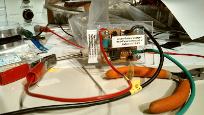
Figure 1:
The charge controller with connecting leads.

Controlling current flow without heat:

Here's the thing about efficiently switching current on and off:  If you have a switch, you need to have it firmly "on" so that the current flowing through it doesn't generate heat due to resistance - and a high-current power FET will do this nicely.  The one that I chose had no more than 0.02 ohms of "ON" resistance and with 10 amps, this would produce a measly 2 watts of heat.  Conversely, when the FET is off it isn't passing any current at all so it isn't even thinking about getting hot.

It's in that "in-between" state that the problem lies:  If there is resistance - say, from the FET not being turned on fully - it will immediately get hot and if one can't get rid of that heat, it will be destroyed.  One must switch the FET on and off quickly so that it spends as little time in that "in-between" state as possible.

On my first version of this controller using a TL431, this could happen fast enough that the FET was being turned on/off very quickly, spending too much of its time midway between "on" and "off" and getting hot.  After a few initial attempts to slow things down with the addition of some capacitors and adding a bit of hysteresis using a few resistors, I realized that in order to make it work it would have to get more complicated, so I decided to scrap the initial version for something "simpler."

Instead, I would use a computer!  See the diagram in Figure 3.

At first glance it would seem that the use of a computer was not going in the direction of avoiding complexity, but standing back for a moment let's take a look at what is needed for a simple PIC microcontroller-based solar charge controller:
  • A PIC.  I would use the 8-pin PIC12F683 which has an onboard A/D converter, watchdog timer and clock oscillator.
  • A voltage regulator.  To allow the PIC to run from the 12 volt battery being charged, I would use a 78L05 to provide 5 volts which I would also use as a voltage reference.
  • A power FET.  This would be used to connect/disconnect the solar panel from the battery, depending on the state-of-charge (voltage) on the battery.
  • A status LED.  Just because I could, I decided to use a red/green LED to indicate that the unit was powered up and actually doing something.  Separate LEDs could be used if that's all you have.
  • Other circuitry.  There was a 10-turn potentiometer for voltage calibration, a pair of transistors to drive the FET and a few miscellaneous resistors and capacitors.
The real magic was to be done in software and I decided to make it work like this:
  • Measure the voltage on the battery.
  • If the battery voltage is above 13.8 volts, disconnect the solar panel from the battery and make the status LED glow green.  Wait for at least 1/2 second before doing anything else - such as reconnecting the solar panel for additional charging.
  • If the battery voltage is below 13.2 volts, connect the solar panel to the battery and wait for at least 1/1000th of a second before doing anything else to the battery.  When in this state, make the LED glow red for at least 1/20th of a second (even if the battery was disconnected 1/1000th of a second later) so that even a brief flash would be more visible.
  • Every 5 seconds, the charging switch (FET Q3) would be opened very briefly and the device will measure the solar panel's open-circuit voltage.  If it was too low - which would happen if there was no sun - the unit would stop charging and indicate this to the user by briefly flashing the LED yellow every 2 seconds.
In other words, the unit could immediately (after 1/1000th of a second) disconnect the solar panel from the battery if the voltage on the battery were above the "full charge" voltage, but it would wait for at least 1/2 second before deciding to reconnect the solar panel if the battery were too low.   

(Note:  Practically speaking, R1/R2 and C3 slow the response to the changing voltage somewhat so it probably doesn't respond quite as fast as 1/1000ths of a second.)

Figure 2:
A close-up view of the controller in its protective case.

The reason for the immediate response if the voltage were on the high side would be to minimize the time that the battery and/or the equipment connected to it was exposed to voltages that might be in excess of, say, 14 volts.  If the battery to which the unit is connected, this is unlikely since the capacitance of the battery alone - not to mention the electrochemical processes - would prevent the voltage from increasing too rapidly.

The reason for the 1/2 second delay if the voltage were on the low site would be to allow the battery voltage to settle down when the charging current was removed, but also to prevent the FET from being turned on and off too quickly and too frequently.  As we know from above, if the FET is fully on or off it's not going to generate much heat at all and by minimizing the rate at which it will switch between those states, heat generation can be minimized.

These two thresholds (13.2 and 13.8 volts) weren't chosen by accident.  If a healthy 12 volt lead acid battery ever does reach 13.8 volts, it is guaranteed to be at least mostly (if not fully) charged. If this same battery is allowed to "float" (e.g. no load) at this same charge level, it will take some time to drift back down to 13.2 volts. If the battery still has a bit of charging to do it will rather quickly drop back down to (and below) 13.2 volts - particularly if there is a load.
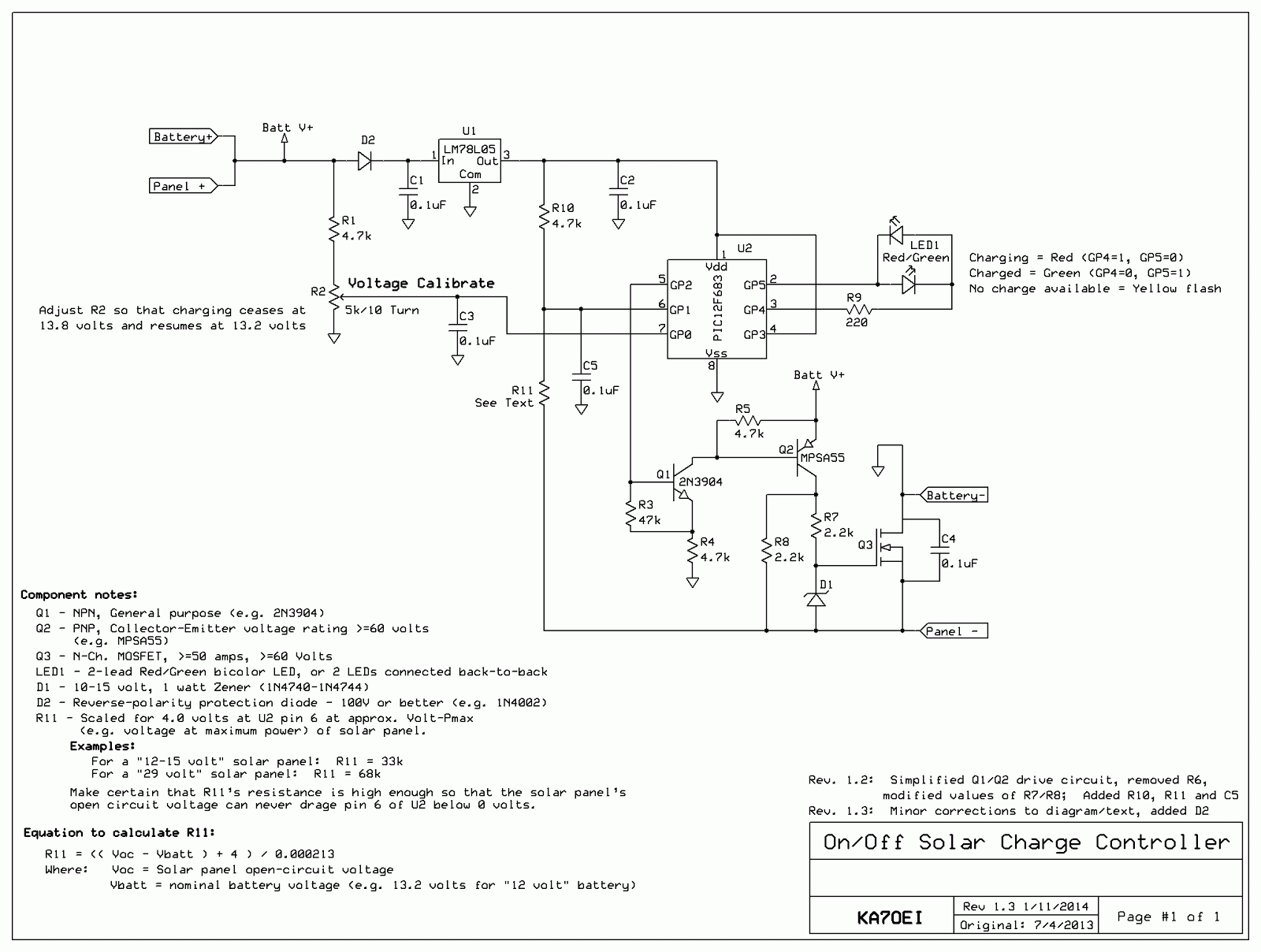
Figure 3.
Schematic diagram of the solar charge controller.  The circuit shown is intended for
"12 volt" (6-cell) lead-acid batteries.
It can be constructed using the PIC12F675 instead - see notes, below.
See notes and text for additional details about this circuit and its use.
Click on the image for a larger version.

So, there you have it, a very simple charge controller!

The .HEX files for programming a processor yourself:

Two .HEX files have been produced:  One for the PIC12F683 as described in the text, and another using the PIC12F675.  These files are NOT interchangeable or likely to be appropriate for other devices.

For the .HEX files, go to the page indicated by the link, below:
  
Web page with .HEX files for solar charge controller  (link)

If you cannot program a processor yourself and are interested in obtaining one, contact me.

Additional comments:

How it's connected to the battery:

As can be seen in Figure 1 large alligator clips are used to connect the battery.  Because the FET switch is in the negative lead, the positive terminal of the battery and the positive terminal of the solar panel are connected together at the battery.  It is recommended that short, heavy leads connect this unit directly to the battery to maximize charge efficiency and to best allow the controller itself to measure the battery voltage:  Long, skinny leads would cause a voltage drop, making the unit "think" that the battery was more-fully charged than it actually was.

A few warnings about the battery connection:

Because there is not extensive protection against high or reverse-applied voltages it is recommended that one connect the charge controller to the battery and then connect the solar panel, and when you are done, do the reverse - disconnect the solar panel then disconnect the battery.

Another extremely important point:  Make certain that the device being powered by the battery is firmly connected to the battery!

Because this device could put the full solar panel voltage across the terminals (in this case, 39 volts) a 12 volt device could be destroyed immediately by over voltage!  If you are using a battery that is in any sort of reasonable condition, this should never happen, but if your battery connections were loose - say, you had alligator clips from the device being powered connected to the battery and you had alligator clips from the charger connected to those clips - and the first set were to accidentally fall off, you could destroy your devices.

It is for this reason that you should always use the "permanent" connections to the battery to connect your devices (e.g. the battery posts.) so that you cannot accidentally have a connection to the solar panel without having the battery in the circuit.

Also, there's no "high-voltage" disconnect to protect the battery and the connected devices should the charge controller accidentally get "stuck" (due to the FET being damaged by lightning, for example) in the "on" state and continually applying current to the battery.  If this were to happen it is likely that the battery could be destroyed by gross over charging and the devices attached to it may be damaged as well.  In this circuit, the FET is reasonably well-protected against such things, certainly not against a very nearby or direct hit!


Explanation of the voltage thresholds:

In software, the battery is connected if its voltage drops below 13.2 volts and is disconnected if the voltage is higher than 13.8 volts:  In between these two voltages, the state is undetermined:  If the voltage had been below 13.2 volts, the panel will be connected (to charge the battery) but if the voltage had been above 13.8 volts, the panel will be disconnected.  Generally speaking, the panel will be connected as soon as the voltage is applied since it is unlikely that a battery that had been sitting for more than a few hours and not connected to a charger as its voltage will likely be well below 13.2 volts.

One could also use this same circuit for charging 6 volt and 24 volt systems as the ratio of the two voltages (on and off) would be correct for lead-acid batteries in this situations, too.  To do this, one may have to select an appropriate value for R1 as well as take into consideration the fact that U1, the voltage regulator, may not operate properly.

For example, at 6 volts unless a low-dropout regulator were used, or one used a different regulator to operate U2 at a lower voltage - say, 3.3-4 volts.  For 24 volts it may be wise to use a regulator that can withstand high voltages (>30 volts) for U1 or put in series with it a 10-15 volt Zener diode, taking care to leave the "top" end of R1 at the battery potential.   If you do change the voltage a which the PIC operates, you'll need to take into account that the voltage scaling resistors (R1/R2 for the battery voltage and R10/R11 used for monitoring the solar panel's open circuit voltage) are appropriately adjusted.

For other types of batteries (e.g. lithium-ion, NiCd or NiMH) this same sort of scheme could also be used, but very different charge-control schemes and voltage thresholds would have to be used to do this safely and this would imply a modification of the code.  Especially if you have several different types of battery chemistries, you may be better off having a small-ish lead-acid 12 volt battery to which these other chargers are connected to function as a low impedance "ballast".

In other words:  Do not use this circuit for any battery types other than lead-acid!

Why switch the panel in/out via its negative lead?

For this design I decided to put the power switching transistor in the negative lead of the solar panel rather than the positive lead and the reason for this is simple:  It was easier to do!

To have put it in the positive lead would have required one of two things:
  • The generation of a "boost" voltage.  I could have used an N-channel FET between the solar panel positive lead and and the battery's positive lead, but I would have trouble driving it.  The reason for this is that in order to turn on an N-channel FET fully, I would need to apply a gate voltage that would be at least 5-10 volts higher than the battery voltage.  Unfortunately, we cannot use the higher open-circuit solar panel voltage for this because if the FET were turned fully on, our solar panel V+ voltage would be the same as the battery V+ voltage.  In order to make this work we'd need to have a circuit that would generate a voltage that was higher than the positive battery voltage.
  • The use of a complementary device.  I could have used an opposite-polarity device such as a P-Channel power FET.  By doing so I could have "pulled down" on the gate/base and turned on the transistor, but there's a problem:  P-Channel FETs are harder to find, a bit more expensive, and typically have higher "ON" resistance than their N-Channel counterparts.  In other words, you can more easily and cheaply find N-channel FETs.
Why use a FET instead of a bipolar transistor in the first place?  Power FETs have the nice property that if you elevate the gate potential far enough "above" the source potential, they essentially turn into a low-loss "on" switch without requiring any drive current.  A bipolar power transistor, on the other hand, would require 1-5 percent (or more!) of the total device current being drawn through its base lead to make it fully conduct, and it would still drop more voltage across it and generate more heat than a FET.

Again, by switching the negative lead of the solar panel I could use a standard N-Channel FET:  Since the source lead of that FET would be pulled down and "away" from the +12 volt terminal of the battery (even to a potential that is negative with respect to the battery minus lead) by the solar panel - and since the PNP driving it was at the battery + potential, we already had a ready-made source of drive voltage for it.

How the circuit works:

U1, a 78LO5 3-terminal voltage regulator supplies a clean source of 5 volts for the microcontroller - and also serves as the voltage reference to determine the charge state of the battery.  The raw battery voltage is scaled first with R1 and then with potentiometer R2, the latter being adjustable so that the "on" and "off" thresholds for charging can be calibrated.

If U2, the PIC12F683 (or PIC12F675) microcontroller sees that the voltage is too low (nominally below 13.2 volts) its sets pin 5 (GP2) high which turns on NPN transistor Q1 which, in turn, pulls "down" on the base of PNP transistor, Q2 to turn it on.  Resistor R4 limits the base current in both Q1 and Q2 while R3 guarantees that if U2's output is in a high-impedance state (such as during startup) that Q1 is turned off by default:  R5 performs a similar function for Q2, respectively as well as speeding up the rate at which it can be turned "off".

When Q2 is turned on, approximately "Batt+" volts (nominally the battery voltage - in the 12-13 volt area) appears at its collector which pulls up on the junction of R7 and R8 which, if the sun is shining, was already at a voltage that is equal to the open-circuit output voltage of the solar panel minus the battery's present terminal voltage:  In the case of the solar panels chosen, the open-circuit, full-sun voltage is around 39 volts so if the battery is at 12.5 volts, the drain of Q3 will have been at -26.5 volts with respect to "ground" - the negative terminal of the battery, or close to the full 39 volts of the solar panel's open circuit voltage.

Pulling the gate of Q3 "upwards" (e.g. making it positive) will turn it on, connecting the negative lead of the solar panel to the negative battery lead.  At this point the gate voltage will drop to about 12-13 volts, but this is sufficient to keep the device chosen fully turned on.  Because the gate-source voltage could conceivably exceed 20 volts or so - the (typical) maximum rating for such a device - at the instant that we turn it on Zener diode D1 in conjunction with R7 form a simple shunt regulator to limit its maximum voltage to a safe level.

Once the voltage rises above 13.8 volts U2, the controller, sets Pin 5 low which turns off Q1 and Q2 and allows R6 to pull Q3's gate voltage down to its source voltage and turn it off, disconnecting the solar panel from the battery.  C4, a 0.1uF capacitor, is placed across the FET so that any "ringing" or transients generated by the FET's being turned on and off are suppressed as well as providing a degree of RFI and static protection.

For this circuit to work properly, Q2 must be rated for the voltages that it will encounter so an MPSA55 was used which has a rating of 60 volts.  Q3 must also be rated for the expected voltage, low "on" resistance and several times the maximum current expected from the panel so a 100 volt, 50+ amp device was used to provide plenty of margin.

The reason for the use of both Q1 and Q2 is so that one can apply the battery voltage to the gate of Q3 when it is "on" to make certain that its resistance (and loss) is as low as possible:  Were Q2 driven directly by U2, we could only attach its emitter to the +5 volt supply and it was turned on, only about 5 volts could have been applied to Q3's gate which, for "normal" N-channel power FETs, may not be enough to drive it into full conduction and minimize its ON resistance.

In looking at Figure 1 and Figure 2 you may note that there is no obvious heat sink on Q3.  In actual operation, with 5-9 amps of current, it ran only very slightly warm but there was plenty of convection coupling (air cooling) as well as heat conduction via the heavy wire (#10-#12 AWG) that was soldered directly to the tab of Q3, its Drain lead which, in turn, connects to the negative lead of the battery.

Added later (after the pictures were taken) is the circuit consisting of R10, R11 and C5.  Forming a voltage divider, this allows the measurement of the voltage across the solar panel when Q3 is turned OFF to determine if there is any usable light falling on the solar panel.  If there is not, the computer will keep the solar panel disconnected and occasionally flash LED1 yellow to indicate that there's presently no power available from the solar panel.  To do make this determination while it is charging (e.g. the LED is red) the panel will occasionally be disconnected for a very brief moment to measure the voltage across the panel.  Of course, if it is not charging (LED is green) it doesn't need to disconnect the solar panel at all to make this reading.

If the panel is being illuminated and Q3 is off, the "Panel -" voltage will go negative with respect to the PIC's ground and via R11, pull U2, pin 6 down from the +5 volt supply   If the voltage on pin 6 of U2 is below about 4.0 volts when the panel is disconnected via Q3 - which indicates that the panel is capable of providing at least some charging current - we know that it is worth attempting to charge the panel.  If the voltage is higher than 4.0 volts when the panel is disconnected via Q3 we can safely assume that there is too little light to bother with and this will put the controller in a mode where it will not attempt to charge the panel and cause the LED to flash yellow every two seconds or so.  (If you have two separate LEDs, both will flash at the same time.)

Calculating the value of R11:

Note that the value of R11 should be chosen for the type of panel to be used.  Nominally, the voltage at pin 6 of U2 should be 4 volts (or lower) at the voltage at which the panel outputs maximum power (this is usually listed in the specs) and R11 should be high enough that at when the panel is open-circuit in full sun, that maximum voltage (often noted as "Voc" in the specs) is not high enough to try to drag pin 6 below ground.

On the diagram are two values shown:  33k for a panel typically used to charge 12 volt batteries directly (e.g. maximum power at around 14-17 volts, 24 volts open-circuit, maximum) and 68k for the panels that we used here (29 volts at maximum power, 39 volts or so open-circuit.)  On the diagram the formula:

R11 = (( Voc - Vbatt ) + 4 ) / 0.000213

Is given.  Since the supply voltage is 5 volts - and we want 4 volts at Pin 6, we want 1 volt of drop across R10 which yields approximately 213 microamps as noted in the above equation.  Kirkhoff's law dictates that the same current must flow through R11 to obtain that same voltage drop across R10 so we add 4 volts to the difference between our expected solar panel open-circuit voltage and get about 31k:  33k is chosen since that is the nearest common resistor value, yielding a "low voltage cutoff" of about 16 volts open-circuit panel voltage.

The "Vbatt" term is one that we must approximate:  If we used precision, fixed resistors for R1/R2 we would know the precise divisor ratio and be able to calculate the battery voltage and subtract it from the open-circuit panel voltage - but since this circuit doesn't do that, we must pick R11 to suit our needs.  In general, if we assume Vbatt to be 13.2 volts, the charge-cutoff circuitry will work fine for a "12 volt" lead-acid battery regardless of its charge state - as long as it is above 6 volts or so since we must have at least enough battery voltage to power our PIC circuit.

Comments:
  • Charging a completely dead battery:  If you were to have this circuit connected to a completely dead battery, charging would never start since the PIC could not be powered from the battery.  Were this to happen - and the solar panel was producing power - one would temporarily connect the Panel - and the Battery - connections together to provide a "bootstrap" charge to the battery.  It may take several minutes for the battery to have enough charge voltage to keep the circuit operational - and this would be true only if the battery was good.  A few warnings if you do this:  Disconnect EVERYTHING ELSE from the battery as it may be bad, and the full panel voltage may appear across the battery if you connect it directly to the panel.  If you do connect the panel directly to the battery in this way, do not walk away - keep monitoring the voltage until it reaches the low-mid 12 volt area.  Finally, be careful when connecting/disconnecting battery connections as sparks may cause hydrogen/oxygen gas explosions.
  • If you were to use a 29 volt panel to charge a 12 volt battery (read below about the efficiency losses in doing so!) there would be no harm in keeping the battery connected if that panel's open circuit were allowed to drop to 16 volts or so - as might happen at dawn/dusk or if the panel were partially shaded or damaged.  At 29 volts, however, the voltage a pin 6 will attempt to go negative, but diodes within U2 will prevent it from going much below -0.6 volts.  While in some cases this excursion beyond the supply rails can cause unexpected effects on the PIC's A/D input MUX and affect other A/D channels, that did not seem to occur in the prototype and it functioned fine - but your results may differ.
  • When in "Inhibit charge" mode (e.g. open-circuit panel voltage too low and charging is discontinued) the prototype, using a 78L05, consumed about 5.5 mA average battery current.  Much of this is the quiescent current of the voltage regulator, but some of it is also the LED occasionally flashing yellow to indicate that it is in a "not charging" mode.  When charging, the circuit will consume around 25 mA, most of this being drawn by the LED and the circuitry that turns on Q3.

Set-up notes:

Setting this circuit up is slightly tricky, but not difficult if instructions are followed.
  • As noted above, please be aware of the hazards associated with high voltage and/or current!
  • Preset R2 to the middle of its range.
  • Connect a variable voltage power supply across the Battery (+) and Battery (-) terminals and set it for 13.20 volts.
  • When first connected, the LED will cycle Green-Red-Yellow if you are using a dual-color LED.  It may then be either a solid color, of flashing.  If it cycles RED-Green-Yellow the LED's leads are reversed!  If you used separate LEDs instead of a single, dual-color LED, both will be on instead of displaying yellow.
  • Make sure that the LED(s) is/are properly connected and/or identified via the power-up color sequence.
    • The colors represent:
      • Red = charging
      • Green = not charging
      • Yellow (brief flash) = Charging voltage not available.
  • With the power supply connected across Battery (+) and Battery (-) set to precisely 13.2 volts, adjust R2 so that the voltage on its wiper (which is also connected to Pin 7 of U2) is 51.6% of the 5 volt power supply's voltage.  If the power supply were precisely 5.0 volts, this would be 2.58 volts.  It is normal for the output of the 78L05 regulator to be between 4.9 and 5.1 volts due to manufacturing tolerances:  It is recommended that you measure it precisely and calculate the 51.6% voltage.  This sets the charge cut-in threshold voltage.
  • If you set the power supply voltage to precisely 13.8 volts, the voltage measured on U2 pin 7 would be 54.0% of the PIC's 5 volt supply voltage, or 2.70 volts.  This is the charge cut-out threshold voltage.
Operation notes:
  • Using the value specified for R11 (33k), if the battery voltage is 13.2 volts and the open-circuit solar panel voltage is below 16 volts, the unit will determine that there is not enough energy from the panel to effectively charge it and in this mode, the LED will be mostly dark, flashing yellow every 2 seconds.  (If you used separate LEDs, they would both light up during the flash.)  Every 5 seconds during charging, the unit will open Q3 and briefly measure the voltage - a process that takes less than 100 milliseconds.
  • If the open-circuit panel voltage is above 16 volts, normal charging will occur with Q3 being closed.  If the battery is discharged and its terminal voltage is below 13.2 volts, the LED will glow red.
  • Once the battery voltage has exceeded 13.8 volts, charging will be stopped, Q3 will be opened and the LED will glow green.
  • Once a battery has achieved full charge, it is normal for the LED to be mostly green, occasionally flashing red - perhaps as often as twice per second.  It is also normal for the voltage to stabilize near 13.2 volts and slowly move upwards over a period of hours or days:  At 13.2 volts, a 12 volt lead-acid battery is "mostly" charged.  Because this controller can only turn charging "on" or "off", it is rather difficult to precisely obtain a charge voltage.
If lead-acid batteries are used other than 12 volt lead-acid, the above steps would be modified accordingly, but note the following:
  • The input to U1, the 78L05, must be at least 6.5 volts for the circuit to work properly.
  • U1 cannot tolerate much above 30 volts, so accommodations must be made if this can happen to protect it.
  • Keep in mind the voltage ratings of Q2 and Q3:  The rating of each should be at least the battery voltage plus the open-circuit panel voltage for a good safety margin.
  • If a different voltage panel is used you will need to properly calculate the value of R11 as noted elsewhere in this text.
  • R2 would be adjusted to 51.6% of the 5 volt supply to set the threshold for the battery voltage  below which charging would be started.  Again, the termination of the charge occurs at 54.0% of the 5 volt supply.  If the battery voltage is increased, it may be convenient to increase the value of R1 appropriately to better-scale the threshold voltages within R2's adjustment span.

"No diode in series with the panel?!?"

It should be noted that there's no "reverse polarity" diode in shown on the diagram as being in series with the controller to prevent the battery's charge from being applied to the panel when the sun is absent.  As it happens, almost all modern, manufactured panels have these diodes built in, anyway - but it would be a good idea to closely check the  panel's specifications.

If, when you connect your panel (shaded from the sun, or in the dark) across your battery and you see more than a few 10's of milliamps flowing into the panel then you might consider adding a series diode to prevent this.

More Comments:
  • While an "MPPT" controller (see the very last section of this article, "By the way, what's an MPPT charge controller?" below, for an explanation) would have been nice, this just wasn't going to happen on such short notice so I threw together a simple "on/off" voltage controller to allow current to be safely thrown at the battery without worrying too much about overcharging it.
  • Charging a battery from a solar panel with a voltage that far exceeds the requirements is very inefficient.  As noted above, if one used a normal "12 volt" panel (those with an open-circuit voltage in the 17-22 volt area) this short of charging is much more efficient.
  • If you build/use this controller for yourself, remember that there are no guarantees that this circuit is either effective or safe.  YOU are responsible for becoming familiar with and implementing the appropriate safety measures and dealing with hazards associated with high voltages and/or currents.
  • Not shown in the diagrams/pictures are necessary fuses and other protection that one must include in a practical installation.


By the way, what's an "MPPT" charge controller?

The charge controller described here simply connect the solar panel to the battery to charge and then disconnects it when the battery has achieved full charge - essentially similar to the "old-fashioned" way solar panel chargers used to work.  Because solar panels act as a source of current, it doesn't really care if its output is shorted out or left open.

Given that our hypothetical solar panel that will output 9 amps at 29 volts we can see that at that voltage we could extract (9 amps * 29 volts =) 261 watts from it, but if we were to short out the panel we would get zero watts (e.g. 0 volts * 9 amps = 0 watts.)

With this on/off switch connecting/disconnecting our battery, we will obviously get 9 amps into the battery, but if the battery were at 13 volts and charging, that would only be (9 amps * 13 volts =) 117 watts of power - this, from a panel that could provide much more than this at a higher voltage.

Clearly we are leaving 144 watts "on the table" somewhere, so how would we make use of it?  One way would have been to charge two 12 volt batteries in series (for 24 volts) which would have yielded 234 watts (e.g. 9 amps * 26 volts assuming 13 volts per battery = 234 watts).  This is much better, but our equipment doesn't actually run on 24 volts and it would be awkward to drag along two 12 volt batteries, anyway.

The way around this is to have an intelligent switching voltage converter.

The way this works is that it has a computer (digital or analog) that will figure out, on the fly, how much current it can pull from the solar panel and automatically calculate the amount of power being pulled at the same time by doing the standards "volts*amps" calculation.


One way to do this is to slightly adjust the switching voltage converter - a circuit that can efficiently convert a higher voltage at lower amperage to a lower voltage at a higher amperage - so that it tries to output a little more current which, in turn, would cause the input to attempt to pull a little more current from the solar panel.  When it does this it does the "Volts * Amps = Watts" calculation of power  and if, when it increased the current being pulled from the panel, it actually did get more power, it would try to pull still more current from the panel, incrementally - but if less power was available, it would decrease the current incrementally to rediscover the optimal condition.  This method is called "Perturb and Disturb" as it constantly "hunts" to dynamically determine the optimal power available from the panel.

If, for some reason, the "volts * amps = watts" calculation showed that there was actually less power available when we attempted to increase the draw from the solar panel by trying to pull too much current and/or the solar panel's output has dropped due to cloudiness, setting sun and/or shading, it would incrementally back off on how much power it tried to pull - and keep doing so until it got to the point at which it, again, got to the maximum output from the panel.

In doing this slight incremental up/down and "feeling" to see if there is more power available from the solar panel, we would be able to extract the maximum amount of power from the panel based on the conditions at that instant.  This type of controller is called an "MPPT" or "Maximum Power Point Tracking" - so called because it constantly adjust itself and tracks the conditions of the charge source (the solar panel) to determine the maximum power that can be extracted from the solar panel and delivered to the load.

[End]

This page stolen from ka7oei.blogspot.com