Showing posts with label PLL. Show all posts

Saturday, February 24, 2024

Repairing a dead Kenwood TS-850S

Recently, a Kenwood TS-850S - a radio from the mid-early 1990s - crossed my workbench.  While I'm not in the "repair business", I do fix my own radios, those of close friends, and occasionally those of acquaintances:  I've known this person for many years and we have several mutual friends.

If you are familiar with the Kenwood TS-850S to any degree, you'll also know that they suffer from an ailment that has struck down many pieces of electronic gear from that same era:  Capacitor Plague.

Figure 1:
The ailing TS-850S.  The display is normal - except
for the frequency display showing only dots.  This error is
accompanied by "UL" in Morse.
Click on the image for a larger version.
This isn't the same "Capacitor Plague" of which you might be aware where - particularly in the early 2000s - many computer motherboards failed due to incorrectly formulated electrolytic capacitors, but rather early-era (late 80s to mid 90s) surface-mount electrolytic capacitors that began to leak soon after they were installed.

The underlying cause?

While "failure by leaking" is a common occurrence in electronics, this failure is somewhat different in many aspects.  At about this time, electronic manufacturers were switching over to surface-mount devices - but one of the later components to be surface-mounted were the electrolytic capacitors themselves:  Up to this point it was quite common to see a circuit board where most of the components were surface-mount except for larger devices such as diodes, transistors, large coils and transformers - and electrolytic capacitors - all of which would be mounted through-hole, requiring an extra manufacturing step.

Early surface-mount electrolytic capacitors, as it turned out, had serious flaws.  In looking at the history, it's difficult to tell what aspect of their use caused the problem - the design and materials of the capacitor itself or the method by which they were installed - but it seems that whatever the cause, subjecting the capacitors themselves to enough heat to solder their terminals to the circuit board - via hot air or infrared radiation - was enough to compromise their structural integrity.

Whatever the cause - and at this point it does not matter who is to blame - the result is that over time, these capacitors have leaked electrolyte onto their host circuit boards.  Since this boron-based liquid is somewhat conductive and mildly corrosive in its own right, it is not surprising that as surface tension wicks this material across the board, it causes devastation wherever it goes, particularly when voltages are involved.

There are some capacitors on the display/driver board on the front panel that should be replaced - but that's not where the majority of the problem lies.

The CAR board - the cause of "display dots"

In the TS-850S, the module most susceptible to leaking capacitors is the CAR board - a circuit that produces multiple, variable frequency signals that feeds the PLL synthesizer and several IF (Intermediate Frequency) mixers.  Needless to say, when this board fails, so does the radio.

They most obvious symptom of this failure is when damage to the board is so extensive that it can no longer produce the needed signals - and if one particularly synthesizer (out of four on the board) fails, you will see that the frequency display disappears - to be replaced with just dots - and the letters "UL" are sent in Morse Code to indicate the "Unlock" condition by the PLL.

Figure 2:
The damaged CAR board.  All but one of the surface-mount
electrolytic capacitors has leaked corrosive fluid and damaged
the board.  (It looked worse before being cleaned!)
Click on the image for a larger version.
Prior to this, the radio may have started going deaf and/or transmitter output was dropping as the other three synthesizers - while still working - are losing output, but this may be indicative of another problem as well - more on this later.

Figure 2 shows what the damaged board looks like.  Actually, it looked a bit worse than that when I first removed it from the radio - several pins of the large integrated circuits being stained black.  As you can see, there are black smudges around all (but one) of the electrolytic capacitors where the corrosive liquid leaked out, getting under the green solder mask and even making its way between power supply traces where the copper was literally being eaten away.

The first order of business was to remove this board and throw it in the ultrasonic cleaner.  Using a solution of hot water and dish soap, the board was first cleaned for six minutes - flipping the board over during the process - and then very carefully, paper towels and then compressed air was used to remove the water.

Figure 3:
The CAR board taking a hot bath in soapy water in an
ultrasonic cleaner.  This removes not only debris, but spilled
electrolyte - even that which has flowed under components.
Click on the image for a larger version.
At this point I needed to remove all of the electrolytic capacitors:  Based on online research, it was common for all of them to leak, but I was lucky that the one unit that had not failed (a 47uF, 16 volt unit) "seemed" OK while all of the others (10uF, 16 volt) had disgorged their contents.

If you look at advice online, you'll see that some people recommend simply twisting the capacitor off the board as the most expedient removal procedure, but I've found that doing so with electrolyte-damaged traces often results in ripping those same traces right off the board - possibly due to thinning of the copper itself and/or some sort of weakening of the adhesive:  While I was expecting chemically-weakened traces, already, there was no reason to add injury to insult.

My preferred method of removing already-leaking capacitors is to use a pair of desoldering tweezers, which are more or less a soldering iron with two prongs that will heat both pins of the part simultaneously, theoretically allowing its quick removal.  While many capacitors are easily removed with this tool, some are more stubborn:  During manufacture, drops of glue were used under the part to hold it in place prior to soldering and this sometimes does its job too well, making it difficult to remove it.  Other times, the capacitor will explode (usually just a "pop") as it is being heated, oozing out more corrosive electrolyte.

With the capacitors removed, I tossed it in the ultrasonic cleaner for other cycle in the same warm water/soap solution to remove any additional electrolyte that had come off - along with debris from the removal process.  It is imperative when repairing boards with leaking capacitors that all traces of electrolyte be completely removed or damage will continue even after the repair.

At this point one generally needs to don magnification and carefully inspect the board.  Using a dental pick and small-blade screwdriver, I scraped away loose board masking (the green overcoating on the traces) as well as bits of copper that had detached from the board:  Having taken photos of the board prior to capacitor removal - and with the use of the Service Manual for this radio, found online - I was confident that I could determine where, exactly, each capacitor was connected.

When I was done - and the extent of the damage was better-revealed - the board looked to be a bit of a mess, but that was the fault of the leaking capacitors.  Several traces and pads in the vicinity of the defunct capacitors had been eaten away or fallen off - but since these capacitors are pretty much placed across power supply rails, it was pretty easy to figure out where they were supposed to connect.

Figure 4:
The CAR board, reinstalled for testing.
Click on the image for a larger version.
As the mounting pads for most of these capacitors were damaged or missing, I saw no point in replacing them with more surface-mount capacitors - but rather I could install through-hole capacitors on the surface, laying them down as needed for clearance - and since these new capacitors included long leads, those same leads could be used to "rebuild" the traces that had been damaged.

The photo shows the final result.  Different-sized capacitors were used as necessary to accommodate the available space, but the result is electrically identical to the original.  It's worth noting that these electrolytic capacitors are in parallel with surface-mount ceramic capacitors (which seem to have survived the ordeal) so the extra lead length on these electrolytics is of no consequence - the ceramic capacitors doing their job at RF as before.  After (later) successful testing of the board, dabs of adhesive were used to hold the larger, through-hole capacitors to the board to reduce stress on the solder connections under mechanical vibration.

Following the installation of the new capacitors, the board was again given two baths in the ultrasonic cleaner - one using the soap and water solution, and the other just using plain tap water and again, the board was patted dry and then carefully blown dry with compressed air to remove all traces of water from the board and from under components and then allowed to air dry for several hours.

Testing the board

After using an ohmmeter to make sure that the capacitors all made their proper connections, I installed the board in the TS-850S and... it didn't work as I was again greeted with a "dot" display and a Morse "UL".

I suspected that one of the "vias" - a point where a circuit traces passes from one side to another through a plated hole - had been "eaten" by the errant electrolyte.  Wielding an oscilloscope, I quickly noted that only one of the synthesizers was working - the one closest to connector CN1 - and this told me that at least one control signal was missing from the rest of the chips.  Probing with the scope I soon found that a serial data signal ("PDA") used to program the synthesizers "stopped" beyond the first chip and a bit of testing with an ohmmeter showed that from one end of the board to the other, the signal had been interrupted - no doubt in a via that had been eaten away by electrolytic action.

Figure 5:
Having done some snooping with an oscilloscope, I noted
that the "PDA" signal did not make it past the first of the
(large) synthesizer chips.  The white piece of #30 Kynar
wire-wrap wire was used to jump over the bad board "via"
Click on the image for a larger  version.

The easiest fix for this was to use a piece of small wire - I used #30 Kynar-insulated wire-wrap wire (see Figure 5) - to jumper from where this control signal was known to be good to a point where it was not good (a length of about an inch/two cm) and was immediately rewarded with all four synthesizer outputs being on the correct frequencies, tuning as expected with the front-panel controls.

Low output

While all four signals were present and on their proper frequencies - indicating that the synthesizers were working correctly - I soon noticed, using a scope, that the second synthesizer output on about 8.3 MHz was outputting a signal that was about 10% of its expected value in amplitude.  A quick test of the transmitter indicated that the maximum RF output was only about 15 watts - far below that of the 100 watts expected.

Again using the 'scope, I probed the circuit - and comparing the results with the nearly identical third synthesizer (which was working correctly) and soon discovered that the amplitude dropped significantly through a pair of 8.3 MHz ceramic filters.

The way that synthesizers 2 and 3 work is that the large ICs synthesize outputs in the 1.2-1.7 MHz area and mix this with a 10 MHz source derived from the radio's reference to yield signals around 8.375 and 8.83 MHz, respectively - but this mix results in a very ugly signal, spectrally - full of harmonics and undesired products.  With the use of these ceramic bandpass filters - which are similar to the 10.7 MHz filters those found in analog AM and FM radios - and these signals are "cleaned up" to yield the desired output over a range of the several kiloHertz that they vary depending on the bandpass filter and the settings of the front panel "slope tune" control.

Figure 6:
The trace going between C75 and CF1 was cut and a bifilar-
wound transformer was installed to step up the impedance
from Q7 to that of the filter:  R24 was also changed to 22
ohms - providing the needed "IF-7-LO3" output level at J4.
Click on the image for a larger version.

The problem here seemed to be that the two ceramic 8.3 MHz filters  (CF1, CF2) were far more lossy than they should have been.  Suspecting a bad filter, I removed them both from the circuit board and tested them using a temporary fixture on a NanoVNA:  While their "shape" seemed OK, their losses were each around 10dB more than is typical of these devices indicating that they are slowly degrading.  A quick check online revealed that these particular frequency filters were not available anywhere (they were probably custom devices, anyway) so I had to figure out what to do.

Since the "shape" of the individual filter's passbands were still OK - a few hundred kHz wide - all I needed was to get more signal:  While I could have kludged another amplifier into the circuit to make up for the loss, I decided, instead, to reconfigure the filter matching.  Driving the pair of ceramic filters is an emitter-follower buffer amplifier (Q7) - the output of which is rather low impedance - well under 100 ohms - but these types of filters typically "want" around 300-400 ohms and in this circuit, this was done using series resistors - specifically R24.  This method of "matching" the impedance is effective, but very lossy, so changing this to a more efficient matching scheme would allow me to recover some of the signal.

Replacing the 330 ohm series resistor (R24) with a 22 ohm unit and installing a bifilar-wound transformer (5 turns on a BN43-2402 binocular core) wired as a 1:4 step-up transformer (the board trace between C75 and CF1 was cut and the transformer connected across it) brought the output well into the proper amplitude range and with this success, I used a few drops of "super glue" to hold it to the bottom of the board.  It is important to note that I "boosted" the amplitude of the signal prior to the filtering because to do so after the filtering - with its very low signal level - may have also amplified spurious signals as well - a problem avoided in this method.

Rather than using a transformer I could have also used a simple L/C impedance transformation network (a series 2.2uH inductor with a 130pF capacitor to ground on the "filter side" would have probably done the trick) but the 1:4 transformer was very quick and easy to do.

With the output level of synthesizer #2 (as seen on pin CN4) now up to spec (actually 25% higher than indicated on the diagram in the service manual) the radio was now easily capable of full transmit output power, and the receiver's sensitivity was also improved - not surprising considering that the low output would have starved mixers in the radios IF.

A weird problem

After all of this, the only thing that is not working properly is "half" of the "Slope Tune" control:  In USB the "Low Cut" works - as does the "High Cut" on LSB, but the "High Cut" does not work as expected on USB and the "Low Cut" does not work as expected on LSB.  What happens with the settings that do NOT work properly, I hear the effect of the filter being adjusted (e.g. the bandwidth narrows) but the radio's tuning does not track the adjustment as it should.  What's common to both of these "failures" is that they both relate to high frequency side of the filter IF filters in the radio - the effect being "inverted" on LSB.

I know that the problem is NOT the CAR board or the PLL/synthesizer itself as these are being properly set to frequency.  What seems to NOT be happening is that for the non-working adjustments, the radio's CPU is not adjusting the tuning of the radio to track the shift of the IF frequency to keep the received signal in the same place - which seems like more of a software problem than a hardware problem:  Using the main tuning knob or the RIT one can manually offset this problem and permit tuning of both the upper and lower slopes of of the filters, but that is obviously not how it's expected to work!

In searching the Internet, I see scattered mentions of this sort of behavior on the TS-850 and TS-950, but no suggestions as to what causes it or what to do about it:  I have done a CPU reset of the radio and disconnected the battery back-up to wipe the RAM contents, but to no avail.  Until/unless this can be figured out, I advised the owner to set the affected control to its "Normal" position.  If you have experienced this problem - and especially if you know of a solution - please let me know.

Figure 7:
The frequency display shows that the synthesizer is now
working properly - as did the fact that it outputs full power
and gets good on-the-air signal reports.
Click on the image for a larger version.

Final comments

Following the repair, I went through the alignment steps in the service manual and found that the radio was slightly out alignment - particularly with respect to settings in the transmit output signal path - possibly during previous servicing to accommodate the low output due to the dropping level from the CAR board.  Additionally, the ALC didn't seem to work properly - being out of adjustment - resulting in distortion on voice peaks with excessive output power.

With the alignment sorted, I made a few QSOs on the air, getting good reports - and using a WebSDR to record my transmissions, it sounded fine as well.

Aside from the odd behavior of the "Slope Tune" control, the radio seems to work perfectly.  I'm presently convinced that this must be a software - not a hardware - problem as all of the related circuits function as they should, but don't seem to be being "told" what to do.

* * * * *

This page stolen from ka7oei.blogspot.com


[END]


Saturday, March 4, 2023

Injection locking cheap crystal "can" oscillators to an external source

Figure 1:
The two generic "can" oscillators tested - both having been
found in my "box of oscillators".
Click on the image for a larger version.

Sometimes one comes across a device with one of those cheap crystal "can" oscillators that is "close" to frequency - but not close enough.  Perhaps this device is used in a receiver, or maybe it's used for clock generation or clock recovery. Such oscillator are available on a myriad of frequencies - although too-often not exactly the right one!

What if we want to "nail" this oscillator to an external (perhaps GPS) reference?  If this oscillator were variable, this task would be simplified, but finding a "VCXO" (Variable-Control Crystal Oscillator) on the frequency of interest is sometimes not even possible.

What if there were a way to externally lock a bog-standard crystal oscillator to an external source?

To answer this question, I rummaged through my box of crystal oscillators (everyone has such a box, right?) and grabbed two of them:  A standard 4 MHz oscillator and a 19.440 MHz oscillator that has an "enable" pin.

Comment:  

This article refers to standard, quartz crystal oscillators and not MEMs or "Programmable" oscillators where the internal High-Q resonating element likely has no direct relationship with the synthesis-derived output frequency.

Injection locking

This is what it sounds like:  Take a signal source of the desired frequency - typically very close to that of the oscillator that you are trying to nail to frequency - and inject it into the circuitry to lock the two together.

This technique is ancient:  It accounts for the fact that a (wobbly) table of pendulum-type metronomes set "close" to the same tempo will eventually synchronize with each other, and it is the very technique used in the days of analog TV to synchronize their vertical and horizontal oscillators to the sync signals from the incoming signal.

It's still used these days, one notable example being the means by which an Icom IC-9700's internal oscillator may be externally locked to an external 49.152 MHz source (see: http://www.leobodnar.com/shop/index.php?main_page=product_info&products_id=352 ) - and this is done by putting a known-stable source of 49.152 MHz "very near" the unit's built-in oscillator.

Injection-locking a discrete-component crystal oscillator is relatively simple:  It's sometimes just a matter of placing a wire near the circuitry (e.g. a "gimmick" capacitor) with the resonant element (e.g. near the crystal or related capacitors) and the light capacitive coupling will cause it to "lock" to the external source - as long as it's "close" to the oscillator's "natural" frequency.

Getting a signal inside the oscillator

Injection locking often needs only a small amount of external signal to be applied to the circuit in question - particularly if it's inserted in the feedback loop of the resonant circuit, but what about a "crystal can" oscillator that is hermetically sealed inside a metal case?

Figure 2:
Schematic depiction of power supply rail
to get the external signal "into" the can.
Click on the image for a larger version.
Because, in many cases, opening the can would compromise the seal of the oscillator and expose the quartz element to air and degrade it, this isn't really an option.  Another possibility would be to magnetically couple an external signal into the circuitry, but owing to a combination of its small size and the fact that these devices are typically in ferrous metal cans, this isn't likely to work, either.

So what else can one do to get a sample of our external signal inside?

Power rail injection

The most obvious "input" is via the power supply rail.  Fortunately - or unfortunately, depending on how you look at it - these oscillators often have built-in bypass capacitors on their power rails, putting a low-ish impedance on the power supply input - but this impedance isn't zero. 

Figure 3:
Top - The signal riding on the voltage rail
Bottom - The locked output of the oscillator
Click on the image for a larger version.
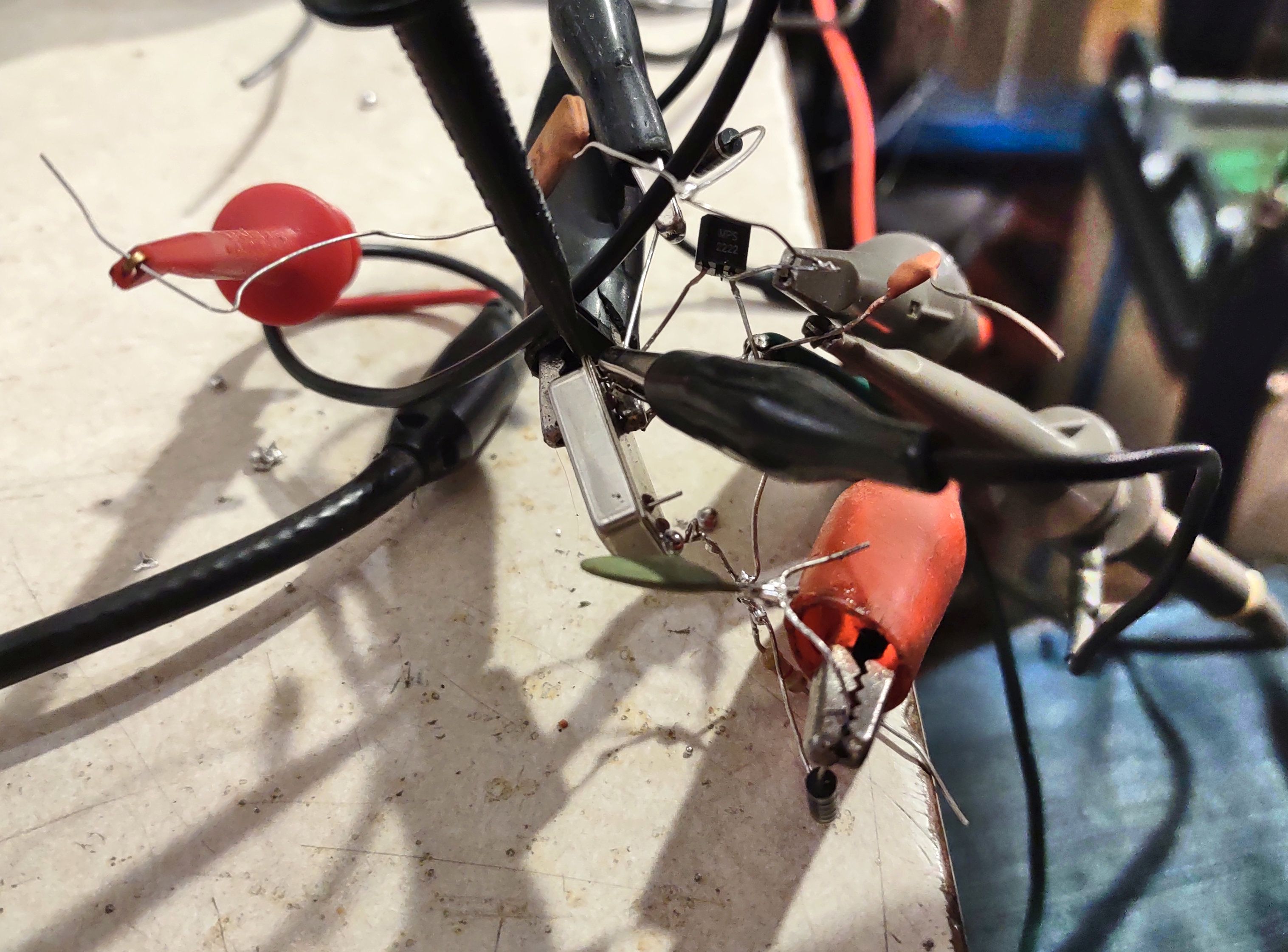
A simple circuit to do this is depicted in Figure 2.  The way it works is by decoupling the power supply via L1 and C1 and heavily "modulating" it with the signal to be locked with Q1.  For the test circuit seen in Figures 2 and 4, L1 and L2 were 10uH molded chokes, C1 and C2 were 0.1uF capacitors and Q1 was a 2N3904 or similar NPN transistor.  

When an external signal is applied to Q1 via C2 (I used +13dBm of RF from a signal generator) Q1 will conduct on the positive excursions of the input waveform, dragging the power supply voltage to the oscillator down with it.  With this simple circuit, Q1 has to dissipate quite a bit of power (the current was about 500 mA) and this action results in a fair bit of power dissipation, likely due to the fact that the bypass capacitance within the oscillator is shunting the energy and causing a significant amount of power to be lost.

This circuit has room for improvements - namely, it's likely that one could better-match the collector impedance of Q1 with the (likely) much lower impedance at the V+ terminal of the oscillator - possibly using a simple matching circuit (L/C, transformer, etc.) to drive it more efficiently.

Figure 4:
The messy test circuit depicted in Figure 2 used to inject the
external into the "can" oscillator via the power pin.
Click on the image for a larger version.

Despite its simplicity, with the circuit in Figure 2 shows how I was able to inject an external signal source into the oscillator and, over a relatively narrow frequency range (15 Hz for the 4 MHz oscillator, 60 Hz for the 19.44 MHz oscillator) it could be locked externally.

The oscillogram in Figure 3 shows the resulting waveforms.  The top (red) is the AC-coupled power supply rail for the oscillator showing about 2 volts of RF imposed on it while the bottom rail shows the square-ish wave output of the power supply.  Using a dual-trace scope, it was easy to spot when the input and output signals were on the same frequency - and locked - as they did not "slide" past each other.

As you might expect, the phase relationship between the two signals will vary a bit, depending whether one is at the low or high frequency end of the lock range and with changes in amplitude, so this - like about any injection-locking scheme - shouldn't be confused with a true "phase lock".

Is the lock range wide enough?

The "gotcha" here is that these are inexpensive oscillators, likely with 50-100 ppm stability/accuracy ratings meaning that they are going to drift like mad with temperature and applied power supply voltage.  What this also means is that these oscillators are not likely to be "dead on" frequency, anyway.

To a degree, their frequency can be "tuned" by varying the power supply voltage:  A 5-volt rated "can" oscillator will probably work reliably over a 3.5-5.5 volt range, often changing the frequency by a hundred Hz or so:  The 19.44 MHz oscillator moved by more than 1.5 kHz across this range, but never getting closer than 2 kHz above its nominal frequency - but this correlates with the often-loose specifications of these devices in terms of frequency accuracy, not to mention temperature!

If your oscillator is "close enough" to the desired frequency at some voltage - and it is otherwise pretty stable, this may be a viable technique, but other than that, it may just be a curiosity.  If one chooses an oscillator with better frequency stability/tolerance specifications - like a TCXO - this may be viable, but testing would be required to determine if a TCXO's temperature compensation would even work properly if the power supply voltage were varied/modulated with an external signal.

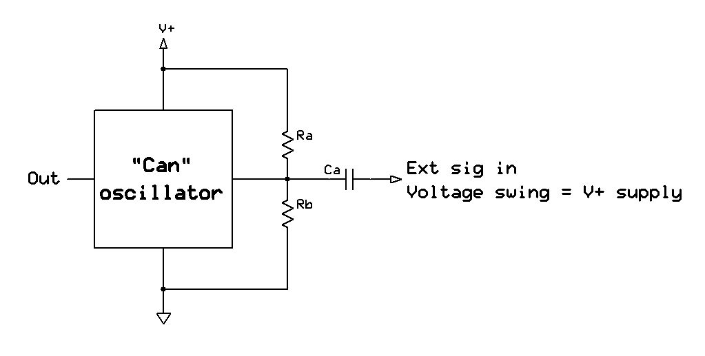
"Enable" pin injection

Figure 5:
Schematic depicting applying an external signal via the
"enable" pin.  The amplitude of the external signal must
have a peak-to-peak voltage that is a significant percentage
of the power supply voltage.
Click on the image for a larger version.
Many of these "can" oscillators have (or may be ordered with) an "enable" pin which turns them on and off - and unlike the power supply pin, this typically has pretty low parasitic capacitance compared to the V+ pin of the oscillator and it can provide a way "in" for the external frequency reference.  Figure 5 shows how this can be done.

For this circuit, resistors Ra and Rb (which may be between 1k and 10k, each) bias the "enable" pin somewhere around the threshold voltage and capacitively couple the signal - in this case, a +13dBm signal from a signal generator which had about 2 volt peak-to-peak swing.  If a logic-level signal is available, one can dispense with the bias resistors and the capacitor and drive it directly.

Note that some oscillators have a built in pull-up or pull-down resistor which can affect biasing and the selection of resistors should reflect that:  If its specs note that the pin may be left open to enable (or disable) the oscillator, this will certainly be the case.  If a pull-up resistor is present, the value of the corresponding external pull-down resistor will have to be experimentally determined, or "Rb" (in Figure 5) may be made variable using a 10k-100k trimmer potentiometer.

The 19.44 MHz oscillator shown in Figure 1 has such an enable pin and by injecting the 2 volt peak-peak signal from the external source into, it will reliably lock over a 900 Hz range.  Some degree of locking was noted even if the signal was quite low (around 250 mV peak-peak) but the frequency swing was dramatically reduced.  For optimal lock range it's expected that a swing equal to that of the supply rail would be used.

The precise mechanism by which this works is unknown:  Does the "enable" pin actually turn the oscillator on and off, does it simply gate the output of the oscillator while it continues to run or is it that this signal gets into the onboard circuitry and couples into the oscillator's feedback loop?  I suspect that it is, in most cases, the former as the "enable" pin often reduces power consumption significantly by completely turning off the oscillator section which would explain why it seems to work reasonably well - at least with the oscillators that were tested.

If the oscillator itself is "gated" (e.g. turned on/off) by the "enable" pin, then this is precisely the mechanism that we would want to inject an external signal into the oscillator.  In looking at the output waveform, however, I suspect that the answer to this question isn't that simple:  If it were simple logic gating one would expect to see the output waveform of the oscillator gated - and mixing - with the external signal once the latter was outside the "lock" range - but this was not the case for the oscillator tested.  I suspect that there might be some sort of filtering or debouncing in the gating circuit, but based on the ease by which locking was accomplished using this oscillator, there was clearly enough of the external signal getting into the oscillator portion itself to cause it to lock readily.

As noted previously, while the lock range was about 900 Hz, the oscillator itself was about 2.5 kHz high, anyway, so it could not be brought precisely onto the nominal frequency.  Again, it may be possible to do this with a TCXO equipped with an "enable" pin, but testing would be required for any specific oscillator to determine if this is viable.

"Locked" performance

The testing of spectral purity using either of these methods was only cursorily checked by tuning to the output of the oscillator with a general-coverage receiver and feeding the resulting audio into the Spectran program to see a waterfall display.  This configuration allows both the absolute frequency and the lock range to be measured with reasonable accuracy.

It can also tell us a little bit about spectral purity:  If there was a terrible degradation in phase noise, it would likely show up on the waterfall display - but when solidly locked, no such degradation was visible.

Although it wasn't tested, it's also likely that locking the oscillator - particularly using the "enable" pin - could be used to "clean up" an external oscillator that is somewhat spectrally "dirty" owing to the rather limited lock range and high "Q" of the "can" oscillator.  This is most likely useful for higher-frequency components (e.g. those farther away from the carrier than a few kHz) rather than close-in, low-frequency phase noise - a property which the most inexpensive oscillators likely don't have is anything resembling stellar performance, anyway.

Harmonic locking?

One thing that I did not try (because I forgot to do so) was harmonic locking - that is, the injection of a signal that is an integer fraction of the oscillator frequency (e.g. 1 MHz for the 4 MHz oscillator) - perhaps something to try later?

Is this useful for anything?

I had wondered for some time if it would be possible to lock one of these cheap oscillators to an external source and the answer appears to be "yes".  Unfortunately, most crystal oscillators have accuracy and temperature stability specifications that cause its natural frequency variance to exceed the likely lock range unless one gets a particularly stable and accurate oscillator.

If one presumes that the oscillator to be "tamed" is good enough then yes, it may be practical to lock it to an external source - particularly via the "enable" pin.  In many cases, such oscillators don't have this feature as they need to be active all of the time so it may be necessary to replace it with one that has an "enable" pin - and then one must hope that the replacement will, in fact, be stable/accurate enough and also capable of being locked externally - something that must be tested on the candidate device.

So the answer is a definite "Yes, maybe!"


This page stolen from ka7oei.blogspot.com

[END]


Sunday, December 20, 2020

Locking the Icom IC-910H to an external 10 MHz (GPS) reference

In late 2009 my friend Bryan, W7CBM, came to me with a project that he had in mind:  "Can we lock my Icom IC-910H to my 'Z-box'?" - in other words, could the 10 MHz output from his Z-3801 GPS Disciplined Oscillator - known to be accurate to better than one part in 100 million - be used to lock his tri-band (2 meters, 70cm and 23cm) all-mode radio to frequency?

Figure 1:
The front panel of the modified Icom IC-910H.
Click on the image for a larger version.

During the initial discussion he'd brought with him an article where Rex, VK7MO, had done a similar thing (see the article on the VK3HZ site from the web archive - link) using an external box to provide a precise version of the radio's 30.2 MHz reference - but he wanted it to be contained entirely within the radio.  

In looking at the requirements and designing the circuit in my head, I decided that we could make it simpler, smaller and easier to use - and with these ideas in mind, I wrote down the specifications for a 30.2 MHz fundamental-mode crystal and he sent an order off to International Crystal.

About 2 months later - in early 2010 - we got back together in my ham shack, crystal in hand, and it was then that I decided that I'd better get around to designing the circuit, so I scribbled the vestiges of a schematic onto a piece of paper and built several circuits that would fit into the aluminum box that Bryan had milled out. At the end of about 3 hours we had a circuit that would faithfully lock the 30.2 MHz crystal oscillator to a 10 MHz external source.  This circuit was fairly small and consisting of two boards:  The amplifier/counter/PLL section wired on prototype board while the VCXO itself was constructed "dead bug" on to a piece of copper-clad PC board material as seen in Figure 3.

"Patience is a virtue - but this is ridiculous!"

And that was where it stopped.  In a case of "out of sight, out of mind", "other fish to fry" - or any number of other excuses - the partly-completed lock unit stayed on a shelf in Bryan's ham shack for a decade, in plain sight.  When I'd go over to his shack, I'd see it as a reminder of a project yet to be completed, but it had become a fixture and was often overlooked.

Until recently.

As it happened, we both had more time available with the onset of winter and we carved out Wednesday evenings to get together to work on various projects and this, being the most senior and nearest completion, came to the top of the pile.  Over the course of a couple evenings we worked on it, having to pause occasionally to get a part, modify some aspect the circuit's implementation, do some physical machine work, or because we ran out of time - but it is now complete!

How it works:

The schematic diagram is depicted in Figure 2, below.

Figure 2:
The schematic of the lock unit for the IC-910H.  This schematic is a reverse-engineered  version of the (now lost) originals and is likely to be mostly correct.
Click on the image for a larger version.

The VCXO:

The heart of the unit is Y201, a 30.2 MHz fundamental mode crystal in a Colpitts oscillator.  Using D201, a varactor diode (approx. 5-20pF) its frequency is made variable, the center of the electronic tuning range being adjusted by trimmer capacitor C201.  The output of the oscillator is buffered by emitter-follower Q202 to isolate the oscillator from the load.

The 30.2 MHz output goes two places:  To Q103, the 30.2 MHz amplifier, and also to a low-pass filter consisting of C208, L201 and C209 which is then output to the IC-901H's synthesizer.

The 10 MHz chain:

Figure 3:
The lock unit under test prior to installation in the case.
Unfortunately, this is the only picture that I got
of the oscillator portion.  The small PCB is the RF sense
circuit, built using SMD components by Bryan.
Click on the image for a larger version.

The 10 MHz input - which can come from a GPS Disciplined Oscillator (GPSDO), a 10 MHz oven-controlled oscillator (OCXO) or a Rubidium source - is input to and amplified by Q101 to a logic level and buffered by U1a, one section of a 74HC86 quad XOR gate.  

The output of U1a is also applied to a 74HC40103 which is wired as a divide-by-50 counter to yield a 200 kHz output - and this is applied to U2a, a 74HC7474 divide-by-two counter to yield a 100 kHz square wave.

The RF sense circuit:

A sample of the 10 MHz signal from U1a is also applied to the input of Q301, which amplifies it:  This RF gets rectified to DC by D301 and D302 and its presence turns on Q301 which pulls R303 to ground and turns off Q301 which is connected to U301 - a 5 volt regulator that is connected to the +5 volt lead of the original TCXO in the IC-910H:  In this way, the internal oscillator in the IC-910H is enabled when there is no 10 MHz signal, but disabled when it is connected.

Also connected to the emitter of Q301 is PNP power switch Q203 which, when R208 is pulled to ground when Q301 turns off, applies power to U201 - a 9 volt regulator - to power up the 30.2 MHz oscillator when the external 10 MHz source is applied, preventing both oscillators from being turned on at the same time.

The Harmonic mixer: 

A sample of the 30.2 MHz signal applied to Q103 is amplified and applied to U1b, another XOR gate buffer, which is then applied, along with the 10 MHz from U1a, into U1d - yet another XOR gate.  This gate acts as a harmonic mixer:  By virtue of the multiplying action of the XOR gate, the 3rd harmonic of the 10 MHz input mixes with the 30.2 MHz input and at the output of this gate is a small amount of the difference frequency - 200 kHz - which easily is filtered by L101 and C103 and amplified by Q102.

Figure 4:
The unit in place - final test.  SMA connectors are used for
10 MHz input and 30.2 MHz output and
feedthrough capacitors are used for the 13.8 volt DC
input and the switched 5 volts for the TCXO.
Click on the image for a larger version.

The use of a harmonic mixer is a very old technique and it has an advantage of simplicity over a more "conventional" digital divider network - albeit more "analog".

A more "conventional" way of doing this might be to divide both the 30.2 MHz and 10 MHz signals down to a common sub-multiple - say, 200 kHz - but to do so would require both a divide-by-50 (to take the 10 MHz down to 200 kHz) and a divide-by-151 (to take the 30.2 MHz down to 200 kHz).  This method works, but adds the a bit of hardware (an additional divider) and, more importantly, these divider steps and subsequent comparisons reduce the PLL loop gain.

By contrast, directly using the 3rd harmonic of the 10 MHz reference to mix with the 30.2 MHz, the 200 kHz difference (ultimately 100 kHz - see below) may be used directly - and loop gain preserved, potentially improving PLL performance and simplifying the design.

The comparison with the reference frequency:

The 200 kHz "difference" signal from the harmonic mixer, filter and amplifier is applied to the divide-by-to circuit U2d to yield to yield a 100 kHz square wave.  The 100 kHz square wave from the divided-down 10 MHz reference signal and that from the 100 kHz "difference" signal are applied to U1c, an XOR gate, which is used as a phase detector.  As the phases of the 100 kHz from the reference signal and that of the difference signal "slide" past each other, the voltage - smoothed by R107 and C107 - will vary from 0 to 5 volts.  If, as an example, C201 in the 30.2 MHz crystal oscillator is adjusted so that 2.5 volts applied to the "VCXO Tune" line, this will cause the crystal oscillator to lock to the reference when the two signals are 90 degrees apart, being steered back onto frequency if they start to drift apart.  

I chose to use an XOR gate as a phase detector over a conventional phase/frequency detector because other than the desired DC component, the lowest-frequency component from its output cannot be lower than the comparison frequency - 100 kHz in this case, with the vast majority of the energy being 200 kHz and harmonics.  In comparison, many of the flip-flop phase/frequency detectors tend to output "occasional" pulses at very low frequency when at/near lock, which are nearly impossible to filter out.  There is a minor penalty, though:  An XOR gate phase detector requires use of 50% duty cycle square waves to work most efficiently, so each of its inputs is divided-by-two by a single 74HC74 dual flip-flop.

Figure 5:
Power connection to the original TCXO - L511 was removed.
Click on the image for a larger version.

Interfacing to the IC-910:

Switching the internal oscillator:

Bryan's IC-910 has the standard TCXO - X512 (the "CR-452") rather than the "High Stability" option (the "CR-293").  Either unit operates at 30.2 MHz, but there is a difference:  The standard TCXO operates from 5 volts while the high stability unit operates directly from the 13.8 volt supply.  Because the internal oscillator must be disabled when another source is applied, one will need to do one of two things, depending on how the radio is configured:

  • Because this radio had the standard TCXO (CR-452 a.k.a. X512), inductor L511 (on the IC-910H's PLL board) was removed to make the power externally switchable and L510 and C501 (the "L510" on Figure 2, above) was connected to power X512.  It is this voltage that is switched by Q303 and regulated by U301 to provide switchable 5 volts.
  • If the "High Stability" option ("CR-293") had been present (as described in the VK7MO case) we would have interrupted the 13.8 volt supply at C511/C512 (on the IC-910H PLL board) and switched it using Q303 directly rather than regulated to 5 volts by U301.  Comment:  It is unknown how much current the high stability oscillator consumes so a slight modification of the Q302 circuit might be required to do this.

Another difference between the way the two oscillators are interfaced appears to have something to do with the output level.  The standard TCXO outputs an RF signal of about 1.2 volts peak-to-peak while it can be seen from the IC-910H service manual that R515 is in series with the output of the high stability oscillator - presumably to reduce its level.

Injecting the locked 30.2 MHz signal:

Figure 6:
Connection of the 30.2 MHz to the PLL board showing
 the added D501 and L502.
Click on the image for a larger version.
Initially we simply connected the external 30.2 MHz in parallel with the output of the original TCXO, hoping that it would go "Hi-Z" when it was powered down - but that did not work:  When the original oscillator was powered down, its output was effectively shorted to ground, dropping the 30.2 MHz signal down to about 100 millivolts, so this signal was applied, instead, to the junction of variable resistor R570 and R572, using R570 to isolate it from the powered-down oscillator.  For this reason, diode D501 was implemented:  This diode - and L502 to provide a DC return - are connected directly at the junction of R570/R572:  When the external reference is activated, diode D501 is biased via R207, turning it on and connected the output of the 30.2 MHz VCXO to the IC-910H's PLL circuit.

If the external reference is not activated, Q203 - the VCXO power switch - is off and no voltage is applied to diode D501 via R207 and it remains "off", effectively isolating the original oscillator from the powered-down VCXO:  By placing the diode at the end of the coax, farthest from the external reference, there is minimal effect on the signal by that coax to the IC-910H's internal oscillator when the external reference is not being used.

Mechanical installation within the IC-910H:

Figure 7:
The back panel of the modified IC-910H.  The added BNC
connector is in the lower-left corner - the location of the
original ground screw, now relocated to the opposite corner.
Click on the image for a larger version.
Bryan had machined the box out of a chunk of aluminum back in 2010, sizing it to just fit (in all three dimensions) on the lid of the PLL unit.  As originally equipped, there are two brackets screwed down to the lid - apparently for the mounting of an optional voice synthesizer and DSP board - but these brackets were removed to make room.  Two SMA connectors were then mounted to the new box - one for the 10 MHz input and the other for the 30.2 MHz output, into the PLL board.  A pair of 1000pF feedthrough capacitors provide passage for the DC power into the box and the switched 5 volt output to the original TCXO on the PLL board.

Not shown (because I forgot to take the photo) is the connection to the switched 13.8 volt supply:  This was connected to the same point on the PLL board as depicted in the VK7MO document mentioned above - except, of course, that the trace did not need to be cut as would have been necessary to switch the power if the high-stability oscillator had been fitted.

The hole on the rear panel for the ground post was drilled out to permit mounting of a single-hole BNC connector with an already-fitted cable with attached SMA connector as can be seen in Figure 4.  This location for the BNC connector was slightly problematic as it somewhat blocked the screw to hold down the cover, but maneuvering of the connector, the use of tweezers and a small-diameter screwdriver permitted its installation.  In the opposite corner (the far-right in Figure 7) a new hole was drilled and tapped for the grounding post.

Spectral purity:

There was a small of concern that the spectral purity of the transceiver with the new reference oscillator would be worse than the original as I'd made no attempt to construct a very low noise oscillator (e.g. a lightly-loaded Butler or similar) so I compared the spectrum with both the internal oscillator and the "new", externally-locked oscillator on the various bands  - particularly on 23cm.

Figure 8:
Transmitter spectrum +/-500 kHz of a CW
carrier on 23cm as seen on an HP-8562A.
Click on the image for a larger version.


On 2 meters and 70cm, very weak (-70dBc) spurs at +/- 200 kHz - the main component of the output of the phase detector - were noted, barely above the broadband noise floor of the transmitter itself - but these were pretty much absent on 23cm as can be seen in Figure 8.  If these had been of concern, it would have been easy to further-improve the loop filter - which is currently a very simple R/C design as evidenced by Figure 2.  The fact that the plot in Figure 8 was made with the analyzer's resolution bandwidth set to 300 Hz should be an indication as to how low these 200 kHz components really are!

Another possible concern was closer-in phase noise:  Would various noise sources of the new circuits (VCXO phase noise, counter jitter, 1/F noise from regulators, loop noise, etc.) cause notable degradation?

Figure 9 gives a clue:  For this test, trace "A" is the original TCXO and trace "B" (the slightly fainter one corresponding with the peak on the right) was produced using the new, externally-locked reference.  As can be seen, the "close-in" phase noise performance of this radio isn't super great, anyway, but the two "noise humps" on either side of the carrier appear to be identical.

This trace also shows a slight difference in frequency, with the original TCXO (the peak on the left) being slightly low in frequency compared to the GPS-referenced, externally locked version - both showing identical amounts of phase noise indicating that the IC-910H is not degraded by this addition.

Figure 9:
A comparison of the close-in phase noise
using the original TCXO (left peak) and the
new, externally locked oscillator (right peak).
Click on the image for a larger version.
Conclusion:

Even thought it has been a long time in the making, this project is complete - and working as well as we hoped that it would.  I'm gratified that a mere decade ago, the circuit that I scribbled onto a piece of paper - and then built in one evening works just as it was expected, with no significant modification!

* * *

 P.S.  Alas, if you wanted to order a crystal, yourself, International Crystal Mfg. is no more, but custom crystals are still available via Quartslab - link, and Krystaly - link - to name but two places.

NOTE:  "Quartslab" stopped doing business in 2021 and "Klove" appears to have acquired the business - link.

(You would have to check with your chosen manufacturer to see if they will make a 30.2 MHz fundamental crystal, though - either that or modify the oscillator to use a 3rd overtone crystal.)

Comment:  Since this article was originally published, devices like the Leo Bodnar GPS reference link have become available that can produce the 30.2 MHz reference required by this radio directly.  This device uses GPS-based timing to set an oscillator to the desired frequency that is programmable - typically with accuracy in the range of 10E-10 or so:  In other words, it can directly synthesize the 30.2 MHz frequency needed by the IC-910H.

If you wish to generate a 30.2 MHz from a stable 10 MHz source that you already have, the Bodnar device really won't help you.

* * *

This page stolen from ka7oei.blogspot.com.

[End]


Sunday, November 1, 2015

Adding FM to the mcHF SDR transceiver

This has been one of those "Rabbit Hole" features.

In the past I have stated several times on the Yahoo Group that I would not be adding FM to the mcHF (a completely stand-alone QRP SDR HF transceiver) any time soon, mostly because I was quite certain that there was simply not enough processor horsepower to do it properly, but quite recently I (sort of) got obsessed with making it work, going from "0 to 60" in just a few evenings of code "hacking".

While it took only an hour or so to get the FM demodulation and modulation working it ultimately took much longer than that to integrate the other features (subaudible tone encode/decode, etc.) and especially the GUI interface with everything!  By the time I was done I'd spent more time than I had hoped (not unexpected!) but at least had something to show for it!

FM on an HF transceiver:

First of all, FM is one of those modes that I have used on HF only a few dozen times in my 30+ years of being a ham - using it most often (albeit rarely) when 10 meters is open and I hear a repeater booming in, but other than that I haven't really had any reason to do so, particularly since there are no local 10 meter repeaters and local activity on "10 FM" is quite sparse.

Figure 1:
Reception of an FM signal as displayed on the waterfall (using the
"blue" palette) showing the sidebands from the 1 kHz tone
modulated onto the carrier being received.  The white background
on the "FM" indicator shows that the (noise) squelch is open.
Click on the image for a larger version.
What might be a practical reason to add FM to the mcHF other than for 10 meter openings or with a transverter (or a modified radio) on a higher band such as 6, 4 or 2 meters where FM is common?  I asked this question on the mcHF Yahoo group and several people noted that in various parts of Europe, FM repeaters and simplex operation on 10 meters is/are (apparently) more common than here in the U.S - not to mention the fact that I suspect that some mcHF users like to hang out on "CB" frequencies where FM is used in Europe.

Background:

As it turns out I was recently adding/fixing some of the current mcHF features, streamlining some code and I decided to look into what, exactly, it would take to demodulate FM.

Before I begin the description it should be noted that the mcHF, in FM receive mode, must utilize "frequency translation" which shifts the local oscillator by 6 kHz - this, to get away from the "0 Hz hole" intrinsic to many SDR implementations that down-convert the RF to baseband:  If we did not do this the FM carrier would land in this "hole" and hopelessly distort it!

With the signal to be received centered at 6 kHz at the input of the A/D converter, a software frequency conversion shifts it back to "0 Hz" where, in the digital domain, the hole does not exist.  True, the FM signal is now modulated +/- zero and includes "negative" frequencies, but since the signals are quadrature and it is just math at this point we can get away with it!

(Note:  The "0 Hz hole" still exists but is now 6 kHz removed from the center of the carrier so it has no effect at all on demodulated signals in receive bandwidths up to 12 kHz.)

The PLL method of demodulating FM:

The most common way to do this is via a PLL, implemented in software
Figure 2:  PLL implementation of an FM demodulator

Depicted in Figure 2 this works by "tracking" the variations of the input signal's frequency using the PLL:  Differences in instantaneous phase are detected, applied to the VCO's tuning line via the Loop Filter.  The loop filter is present to remove the energy from the original carrier frequency, effectively leaving only the audio modulation behind, a sample of which is high-pass filtered to remove the DC content and used to extract the demodulated audio.

In hardware this type of scheme is used in PLL ICs such as the NE564 and NE565, or even the good old 4046 PLL IC:  Many implementations of hardware-based FM demodulators may be found on the internet using these chips!  (Hint:  Google "NE565 SCA decoder").

In software this method would typically be applied in those instances where the "carrier" frequency was high, compared to the highest modulated frequency contained in the FM signal to be demodulated and the "VCO" would be an NCO (Numerically Controlled Oscillator) - essentially a software-based DDS (Direct Digital Synthesis) "oscillator."  In a typical SDR application the implementation would appear more complex than in the above block diagram, using both the I and Q channels as part of the phase detector (and to avoid ambiguity since both are needed to avoid the "frequency image" anyway) - but the intent is quite clear.

Out of curiosity I decided to implement this on the mcHF, but as expected it was to "expensive" in terms of processing power - plus, the "carrier" frequency (in software) was only 6 kHz - not too far above the highest modulated frequency.  I could hear the audio, but it was somewhat distorted.

The "arctangent" method of demodulating FM:

Applying another tactic I went for the "arctangent" method.  If you recall your trigonometry, the arctangent is that number that you get when you input the ratio between the two sides of a triangle to yield the angle.  Related to the arctangent is the "atan2" function that appeared in computer languages where not just the ratio is inputted to the function, but the actual lengths of the sides of the triangle (y, x) and the angle is computed from that.

If we consider the instantaneous amplitudes of our I and Q signals to be vectors, we can see how we can use this function to determine the angle between those two vectors at any given instant - and since FM consists of rapidly changing phases (angles) we can therefore derive about the frequency modulation:  The more the angle changes, the more deviation!  (More or less...)

Figure 3:  Speech-modulated audio being received and displayed
on the "Spectrum Scope" showing the width of a typical
voice-modulated, pre-emphasized FM signal.  The red "FM"
indicator shows that the subaudible tone is being received and
properly decoded.
Click on the image for a larger version.


In order to do this you must know how the vector has changed from one sample to the next, using previous information to do so, so a bit of math is first used to accomplish this as described in the following code snippet:

loop:
   y = Q * I_old - I * Q_old
   x = I * I_old + Q * Q_old
   audio = atan2(y, x)
   I_old = I
   Q_old = Q

Where:
   "I" and "Q" are our quadrature input signals
   "audio" is the demodulated output, prior to de-emphasis (see below.)


Because we supply it with both x and y, "atan2" function has the convenient feature of knowing, without ambiguity, the quadrant from which the two sides of the triangle are derived - something not possible from the normal "atan" function.  For example if our vector is +1, +1 - a ratio of 1 - we know that our angle is 45 degrees in the first quadrant, but if our vector is -1, -1 - our ratio is still 1, but clearly this angle is in the fourth quadrant and the normal "atan" function would give us a completely bogus answer - but "atan2" would faithfully yield the correct answer of 315 (-45, actually) degrees.

If you are coming from the analog world you know that one of the necessary steps in properly demodulating an FM signal is to apply limiting after bandpass filtering, but before the actual FM demodulation - this being a process where incoming signal is typically amplified and then strongly clipped - often several times - to assure that the amplitude of the resulting signal is constant regardless of the strength of the original signal.  The reason for this is that most analog FM schemes are either amplitude sensitive to a degree (e.g. slope detection, the "Foster-Seeley" discriminator - link, or even the so-called "ratio detector" - link) or can operate over only a somewhat limited amplitude range and still maintain "linearity" in their frequency-dependent demodulation.

As it turns out the while both of the aforementioned schemes are amplitude-insensitive with this limiting applied, the "atan2" method can be considered to be the ultimate "ratio detector" in that all it really cares about is the ratio of the vectors from the I and Q channels and not a whit about their amplitudes!  If the signal is reasonably strong, both channels (I and Q) will reflect the instantaneous angle-change of the received signal with respect to the previous sample.  As with any other method of detection of frequency modulation as signals get weaker, noise begins to intrude, causing uncertainty and the calculation of the instantaneous angle begins to be contaminated with random bursts of energy which naturally shows up as "popcorn" and/or "hiss" in the recovered audio.

Rather than using the compiler's rather slow, built-in floating-point "atan2()" function I decided to use the "Fixed point Atan2 with Self-Normalization" function (in the public domain) attributed to Jim Shima posted (among other places) on the DSP Guru Site (link here).  Actually, this algorithm was quite familiar to me as I'd unwittingly derived a very similar method many years ago on a PIC-based project in which I needed to do an ATAN2-like function using integer math to derive the bearing on a direction-finding (DF) system. (The DF system is described here - link)

Needless to say, this algorithm is blazing fast compared to the built-in, floating-point "atan2" function and demodulating FM with this much horsepower simply would not be possible without its "cost savings" and the accuracy of the result easily yields sub 1% THD (distortion) - more than adequate for communications-grade FM.

De-emphasizing the demodulated audio:

The audio that spits out of the "atan2" function is proportional to the magnitude of the frequency deviation at any modulated frequency (within reason, of course!) - but in amateur radio, at least for voice communications, we do not use "FM" per se, but rather "Phase" modulation (PM).  Without going into the math, the only thing that you need to know is that in order to use an FM modulator to generate a PM-compatible signal one must "pre-emphasize" the frequency response of the audio at a rate of 6 dB/octave.  In other words, if you were set a signal generator to produce +/- 2 kHz of deviation with an audio signal of 1 kHz, if you change that audio signal to 2 kHz - but kept the audio level the same - the deviation would increase to +/- 4 kHz of deviation when you are using PM.

If you did not do this pre-emphasis, your audio would sound muffled on an ordinary amateur "FM" receiver.  Conversely, if you use an "FM" receiver for the reception of PM you must apply a 6 dB/octave de-emphasis to it:  Without this the audio tends to sound a bit "sharp" and tinny.

There is a practical reason for doing this and it is in the form of "triangle noise" - that is, as an FM signal gets weaker, the recovered audio does not get quieter, but it gets noisier, instead, with the noise appearing in the high frequencies first as high-pitched hiss.  By using "PM" (or more typically, "true" FM with pre-emphasis on transmit and de-emphasis on receive) we reduce the intensity of this high-pitched noise on weaker signals:  Since we are boosting the "highs" on transmit and then reducing them back to normal on receive, those audio frequencies that would be first affected by noise as the signal weakens are maintained at higher levels while at the same time reducing the amplitude of the high frequencies in which the noise will first appear, preventing the phenomenon by which the high frequency component would otherwise be the first to disappear into the noise with weak signal.  The end result is that with PM, the signal can be weaker - and seem to be noise free - more than is possible with "straight FM".

For an explanation of noise in FM signals, in general, read the page "Pre-Emphasis (FM) Explained" - link.

In an analog circuit this de-emphasis is as simple as an "R/C" (resistor-capacitor) low-pass filter (series resistor followed by a capacitor to ground) and it may be simulated in code as follows:

loop:
  output = old + α * (input - old)
  old = input

Where:
   "α" is the "smoothing" parameter
  "input" is the new audio sample
  "output" is the low-pass (integrated) audio data

In the above, the output data is proportional to the previous output and the next input which means that as the rate-of-change increases, the output decreases - effectively forming a single-pole low-pass filter of 6 dB/octave.

If you were to implement this with real components (resistor, capacitor) you would not select them for really low frequency as this would mean that by the time you got to speech frequencies (1-2 kHz) your audio would rolled of by many dB - but this would also mean that low-frequency components (subaudible tones, AC hum, even the low-frequency components of noise) would seem to be artificially amplified and could "blast" the speaker/amplifier.  Instead, one would select a "knee" frequency above which one would start to roll off the audio - typically just below the bottom end of the "speech" range of 300 Hz or so and by doing this the low frequencies are not as (seemingly) amplified as they would by otherwise.  As it turns out, with an "α" setting of 0.05 or so we can achieve a reasonable (low frequency) "knee" frequency at a sample rate of 48 kHz.

Even if we appropriately select a "knee" frequency as above our audio amplifier/speaker will still get blasted by low-frequency noise since we must still amplify the signal by well over 10 dB to get reasonable amplitudes at speech frequencies, but we can - with a "differentiator" - the inverse of (but similar to) the integrator described above, knock off these low-end components.  In software this differentiator function (which, in the analog world, is a series capacitor followed by a resistor to ground) is performed as demonstrated below:

loop:
  filtered = α * (old_input + input - old_filtered)
  old_filtered = filtered
  old_input = input

Where:
  "α" is the the equivalent of the time constant in that a "small" α implies an R/C circuit with a fast time-constant strongly affecting "low" frequencies.
  "input" is the new audio sample.
  "filtered" is the high-pass filtered (differentiated) audio

Setting "α" to 0.96 (with a sample rate of 48kHz) put the "knee" roughly in the area of 300-ish Hz and with the "low-pass" (integrator) and "high-pass" (differentiator) cascaded the low-frequency speech components were minimally affected, but the combination of the "knee" frequency of the integrator and the nature of the differentiator meant that the very low components (below approximately 200 Hz) were being attenuated at a rate of around 12dB/octave - all by using simple filtering algorithms that take little processing power!  Again, it is important that we do this or else the very low frequencies (subaudible tones, the "rumble" of open-squelch noise) would be of very high amplitude and easily saturate both the audio amplifier and speaker, causing clipping/distortion at even low audio levels.

At some point I may attempt to design an FIR or IIR filter that will both de-emphasize the audio at 6dB/octave and filter out the low frequencies used by subaudible tones but I wanted to at least try the above method which was pretty quick, easy to do, and had a fairly low processor burden.

Pre-filtering:

One factor not mentioned up to this point, but extremely important - especially with FM - is that one must bandwidth-limit the I and Q channels before demodulation.  More than in the case of AM, off-frequency signals will contribute to noise and nonlinearity in the demodulation process and it is easy to see why:  If we are simply using vectors with our "atan2" function to recover the frequency modulator, anything that contaminated that information would distort and/or add noise to the resulting audio so it is important that we feed only enough bandwidth to the demodulator to pass "enough" of the signal.

Defining the bandwidth of a modulated FM signal is rather tricky because it is, in theory, infinitely wide. In practice, the energy drops off rather quickly so the "far out" sidebands soon disappear into the noise, but how quickly can we "clip off" the "close in" sidebands?  Clearly, we must have at least enough bandwidth to pass all of our audio, and since the FM signal is symmetrical about its center, it's twice as wide as that.  There is also the issue of the amount of frequency deviation that is used.  If we take our example of +/- 2.5 kHz deviation in "narrow" mode we know that just because of that, alone, our signal must be at least 5 kHz wide!  It would make sense, therefore, that the actual bandwidth of the signal is related to both the amount of deviation and the audio imposed on it - and it does, and this is called "Carson's Rule" and you can read about it here - link.  This rule is:

 occupied bandwidth = 2 * (highest audio frequency) + 2 * (deviation)

If we have +/-2.5 kHz deviation and our audio is limited to 2.6 kHz the calculated bandwidth would be 10.2 kHz.  It should be remembered that this is considered to be the occupied bandwidth of the signal and generally indicates the minimum spacing between similar signal, but it turns out that if we are willing to put up with minor amounts of signal degradation our receive bandwidth may be narrower.  By cutting off a few extra sidebands the result is a bit of added distortion since part of signal that represents the vectors presented to the "atan2" function have been removed and the representation is understandably less-precise.

In the case of the mcHF, filtering for the FM demodulator is done by the same Hilbert transformers that are already present for "wide" SSB and AM demodulation where they can also be configured to provide a low-pass function.  For example, there exist 3.6, 5 and 6 kHz low-pass versions of the Hilbert transformers that provide the 90 degree I/Q phase shift and coupled with the fact that these would operate both above and below center frequency, they yield approximate detection bandwidths of 7.2, 10 and 12 kHz, respectively.  Using a filter wider than 12 kHz (+/- 6 kHz) is problematic in this implementation because, as noted earlier, we are shifting our signal by 6 kHz and with a 12 kHz bandwidth, one edge of the filter actually falls in the "zero Hz hole" of the hardware.  This is not a problem at the 12 kHz bandwidth, but it is a problem at wider bandwidths and can result in significant distortion.

While receive bandwidths more than 12 kHz could be obtained using a shift greater than 6 kHz, testing (both on-the-bench and on-air) has shown that "wide" +/- 5 kHz deviation signals may be received with little/no obvious distortion with the 12 kHz bandwidth setting - and even the 10 kHz setting is very "listenable".

Surprisingly, if you cram a +/- 5 kHz deviation signal through the 7.2 kHz filter, the results are generally quite usable although distortion and frequency restriction are becoming evident and there may be the risk of clamping if the squelch is set too tight.  One advantage of a 7.2 kHz filter over a 12 kHz filter is that the former, being only 60% as wide, will intercept commensurately less noise on a weaker signal which means that it may be possible to gain an extra dB or two of receiver sensitivity by switching to the narrower bandwidth - if one is willing to accept the trade-off of lower fidelity!

In a later posting I'll talk about the squelch "circuit", subaudible tone detection as well as frequency modulation.


[End]

This page stolen from "ka7oei.blogspot.com".