|
| Figure 1: The Renogy RNG-DCC1212-20 - an isolated and current-limited battery charger, intended for use with vehicle electrical systems. Click on the image for a larger version. |
There are times - usually on a camping or road trip - where I would like to charge my LiFePO4 batteries en-route, from the vehicle. The "need" is largely the result of having one of those coolers with a built in compressor: It runs about 10-30% of the time at normal room temperature and pulls up to about 3.5 amps when doing so - but it's also advantageous to be able to keep a battery topped off in the event that you didn't start the trip with a fully-charged battery in the first place.
To do this, one may be tempted to connect the battery directly to the vehicle's electrical system, as might have done in days past with a lead-acid battery.
DO NOT do this with any lithium battery - at least not directly.
In short, you cannot and should not parallel a LiFePO4 battery with an existing charging system intended for lead-acid batteries. The biggest issue with doing so is that unlike a lead-acid battery, a LiFePO4 battery will attempt to charge with all available current, likely resulting in blown fuses, heated wires and burnt-out alternators. A secondary issue has to do with the BMS (Battery Management System) of the LiFePO4 simply disconnecting abruptly when the battery is fully-charge, potentially causing voltage spikes capable of damaging vehicle electronics and possibly, the BMS itself.
See the section "Why you need to treat LiFePO4 batteries differently" in the "tl;dr" section near the end of this article (link) for more details as to the problems that can occur.
A solution
The solution to the issues noted above lie largely in limiting the charging current. One way to do this would be resistively - perhaps with the use of intentionally small-gauge wire and/or resistor or incandescent automobile headlamp in series. This will, by its nature, generate heat as it's inefficient - and it can generate quite a bit of heat (potential fire risk here!) - but this is the way one might have accomplished this in years past.
This sort of limiting may occur unintentionally if one charges via, say, a cigarette lighter/accessory plug connected with light-gauge wire, but this is sort of a "kludge". One issue with this is that it can cause frequent blown fuses as the current isn't regulated and if the user attempts to circumvent this by using a higher-current fuse, damage to the electrical system (or even fire) can result. If the connection is made to a power source that is switched on/off with the ignition, a connected battery can "back feed" the electrical system which can result in the battery being discharged when the vehicle is off or, worst case, damage to both the vehicle and battery.
These days one would use a current-limited and regulated voltage DC-to-DC converter with its power source connected as close to the vehicle battery as possible.
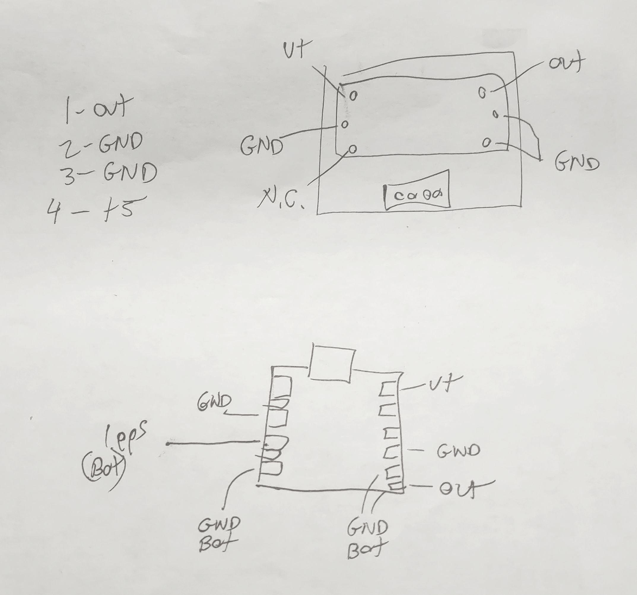
One of the many devices out there that will fit the bill is the Renogy RNG-DCC1212-20 (pictured above), available at the time of the original posting of this article for around US$100: Using DIP switches, the type of battery (lead-acid, Lithium-Ion or LiFePO4 - I configured for the latter) may be selected along with the charging profile/voltage - and the device will limit the maximum charge current to just 20 amps, selectable to 10 amps with the addition of a jumper wire to the "LC" terminal. What this means is that no matter the charge state of the LiFePO4 battery, the current being pulled from the vehicle's electrical system will be limited - very useful if one expects to avoid blowing fuses, destroying alternators, or burning up wiring. (Note: I have no vested interest in Renogy, they just happen to make one of the readily-available devices that is appropriate for this task.)
Additionally, it's rated to operate from between 8 and 16 volts while maintaining a constant output voltage (once the output current has dropped below limiting) that is independent of the voltage from the vehicle's electrical system. The Renogy is also an isolated DC-DC converter in that there is no electrical connection between the input and output terminals: By being isolated, circulating currents (through the chassis or other "sneak paths") can be completely avoided which may be helpful for some sensitive equipment and/or to minimize/eliminate alternator "whine".
This particular unit is rated for up to 20 amps output current. Rated at about 90% efficiency, it will take more power on its input connections than it will output, producing a bit of heat (which is why it has internal fans). Also note that the current pulled by the unit will vary depending on the voltage input despite the fact that the output voltage and current - and overall power consumption - may remain constant.
For example, let's say that the unit is outputting 20 amps at 14.5 volts, representing a LiFePO4 battery that is nearly fully-charged representing an output power of 290 watts: Assuming 90% efficiency, the unit will actually consume 322 watts with the difference (32 watts) as heat. At an input voltage of 12.0 volts, 322 watts is 26.8 amps, but at 14.0 volts, 322 watts is just 23.0 amps. The fact that it can pull more current from the source supply than it is outputting - particularly when the input voltage goes down - must be taken into account when sizing the wire and selecting the fuse rating.
You can't just connect it and walk away!
The Renogy has a "D+" terminal that, when connected to a voltage source, will activate it. The intent is that this wire is connected to some part of the vehicle's electrical system that is likely to be on when the engine is running to charge the battery - such as the "accessory" circuit. The reason for this is that the Renogy itself has no useful low-voltage disconnect: If you connected it to the vehicle's electrical system with the engine off, it will happily attempt to charge the battery to which it's connected - and if the battery being charged is a large, discharged LiFePO4 battery, it will likely run the vehicle's battery down completely in doing so.
One way around this would be to monitor the battery voltage: If it's above about 13.2-13.5 volts, one can be assured that the engine is running, but it will drop fairly quickly when the engine is off as the lead-acid starting battery's voltage drops. Unfortunately, the Renogy's only means of low-voltage cut-off is set to 8 volts (a very "dead" 12 volt battery!) which requires that I come up with another way of enabling/disabling the device.
Another issue is that whenever the unit is on (the D+ line is active) but unloaded (e.g. no battery connected to the output) it consumes about 250 mA at 14 volts - increasing to over 500mA at 10 volts - and more than this if its cooling fans are running: This sort of load may run a battery dead in a few days at best, so there had to be a way of completely disabling it and eliminating current draw.
A voltage-controlled switch
In poking around, I noted that without the "D+" line connected to a voltage source, the Renogy drew no detectable current meaning that I could leave the high-current input leads connected full-time: By switching just the D+ lead I could enable/disable the device as needed without the need of a heavy-duty relay. (Judging by the "clunk" that one hears when applying power to the D+ line, the Renogy probably has such a relay built into it.)
As the D+ line itself drew very little current (only about 3 milliamps) and anything above about 4 volts seemed to reliably trigger it, it would take almost nothing to drive it so the circuit could be very simple as the diagram below shows:
 |
| Figure 2: Schematic diagram of the low-voltage cut-off circuit with hysteresis. This circuit provides an "on/off" control of the converter to the "D+" line based on the voltage at the "V+" and "V-" connections. Click on the image for a slightly larger version. |
How it works:
The "V+" and "V-" lines are connected across the unit's input terminals to monitor the voltage applied to it. Resistor R1 scales the input voltage to a lower value to apply to the top of R2, a 10-turn trimmer potentiometer, that is used to divide the voltage down to the 2.5 volt threshold of U1, a TL431 "programmable Zener" via its "reference" terminal. Capacitor C1 connected across the top of R2 provides a degree of filtering to reduce the probability of the circuit from responding to noise on the electrical system.
 |
| Figure 3: The prototype, built on a scrap of proto board. This uses uses through-hole components, but could have been built to be much smaller using surface-mount devices. The capacitor has been lifted up to allow a better view of the components. Click on the image for a larger version. |
Resistor R3 limits the current into U1 and R4 limits the current into Q1 while R5 keeps the emitter-base voltage of Q1 high when U1 isn't conducting, turning it off, resulting in no voltage on the "Out" lead and in this state, with the Out lead connected to the Renogy's "D+" connection, the unit would be powered down and draw no current. Resistor R6 offers protection to the circuit in case the "Out" terminal is momentarily shorted to ground.
If the voltage on the reference terminal on U1 exceeds 2.5 volts, it turns on, pulling the bottom of resistor R3 toward ground, turning on Q1 and causing the "Out" lead to go high, enabling the Renogy via the "D+" line. When this voltage goes high, resistor R7 feeds back a slight amount of current into the junction of R1/R2, very slightly increasing its voltage, lowering the circuit's turn-off voltage slightly but leaving the turn-on voltage unchanged: The value of 270k shown causes this voltage difference between "on" and "off" to be about 0.9 volts while a value of 680k results in a threshold difference of about 0.3 volts.
This threshold difference between turn-off and turn-on (a.k.a. hysteresis) is very important to the stable operation of this circuit. If the voltage applied to the circuit were just above the threshold (by a fraction of a volt) the "Out" lead would turn on and activate the Renogy. When this happened, the Renogy would start drawing current, causing the voltage to drop slightly through wire losses and load on the electrical system - but if this voltage dropped below the threshold, the "Out" lead would turn off again and the current consumption would stop, causing the voltage to rise again and turn it back on, causing an endless "on-off" cycle.
By adding such hysteresis - and making sure that the voltage drop under load was comfortably less than the hysteresis amount - the unit will reliably turn on at the high voltage threshold and will not turn off until/unless the voltage drops below the low voltage threshold. It is also imperative that this unit be connected as close to the battery (with appropriate fusing!) with as short and heavy leads as practical: Too-light wiring will cause the voltage to drop under load, possibly causing it to trip out due to low voltage - only to be re-enabled immediately (e.g. the "on/off" cycling mentioned above.) The need to minimize voltage drop is one reason why the power source should be connected as near the battery/alternator as practical.
 |
| Figure 4: The completed unit in heat-shrink tube. There are no exposed electrical connections - just the adjustment at the end. Click on the image for a larger version. |
Figure 3, above shows the prototype unit, built on a small piece of prototype board. R2, the 10 turn potentiometer is the blue device on the far right with U1 being the black object to the left of it with Q1 being on the far left. In this photo, capacitor C1 is bent up, out of the way to allow a view of the components underneath where it will be laid over.
Figure 4 shows the same circuit covered with some yellow heat-shrink tubing to hold the components together and to protect it from external short circuits. The end of the adjustment resistor, R2, protrudes from the end of the tubing so that it is accessible.
Installing within the unit
 |
| Figure 5: The circuit within the converter. The DC output terminals (to the battery being charged) are in the lower part of the image. Click on the image for a larger version. |
Figure 6 shows how these wires are routed. In addition to the connection to the "D+" terminal from the circuit, another wire and a switch was added that optionally connects the "LC" terminal to the "D+" to set the Renogy to the "Low Current" mode by pulling it high when the switch is closed - in this case, limiting the maximum charge current to 10 amps, which may be useful if you are connecting the unit to a current-limited power source (e.g. "cigarette lighter" plug) that cannot supply the 25-ish amps current input that the unit may draw when charging at 20 amps output.
 |
| Figure 6: Looking on the "output" side of the Renogy, this shows how the "out" wire from the circuit routes out of one of the air to the "D+" terminal. Also shown is a switch that optionally connects the "D+" to "LC" terminal for just 10 amp max. Click on the image for a larger version. |
This "modification" - since it does not involve drilling any holes - is "reversible" if desired as the circuit and wiring could be easily removed.
In-vehicle testing and use
High/low voltage turn-on/turn-off
Prior to testing the modified unit in my vehicle I set the "cut-in" voltage to about 13.65 volts which resulted in a disconnect voltage of around 12.7 volts - a voltage below which a 12 volt lead-acid battery will quickly drop when charging is stopped. As expected, the unit did not get turned on until a few seconds after the engine was started, the voltage rising due to charging by the alternator: If the battery had been heavily discharged and a lot of accessories were running (headlights, blower, wipers) it may take longer than this for the voltage to rise above the threshold.
The voltage dropped below the 12.5-12.7 volt shut-off threshold within a few 10s of seconds of turning off the engine with the entire unit drawing only about 0.5mA (all of that being from the added circuit) in that state - far lower than the vehicle's own quiescent current, and probably lower than the vehicle battery's self-discharge rate. So far, I have found no tendency for the unit to cycle on and off while the engine is running - even if the headlights, heater blower and windshield wipers are on. (As noted in a sidebar below, cycling did start to occur, but this was traced to the adjustment potentiometer setting having drifted upwards by about 0.4 volts, likely due to vibration.)
Of course, the voltage thresholds mentioned above are only valid for a healthy (and properly functioning) conventional charging with lead-acid batteries as part of the chassis electrical system: If your vehicle somehow has a different type of electrical system than the conventional "alternator + lead acid" configuration it'll be up to you to determine how and even if a solely voltage-referenced on/off system like this can be done.
RF Noise generation
Being an amateur radio operator, I was concerned that this unit might produce an excess of radio frequency interference as it contains a high-power oscillator in its power converter. While visual inspection of the Renogy (with its end covers removed) showed that it does have some filtering of its own in the form of series inductors and capacitors across the input/out leads and to the metal case (to suppress common-mode and differential RF energy) it would be unusual for even a well-designed commercial device to go to extremes in reducing radio frequency energy to the point of extinction.
Using a "Tiny SA" Spectrum analyzer I connected directly to the input and output leads - using a 0.002uF capacitor to block DC and protect the analyzer - I measured the amount of RF energy being differentially emitted from the unit.
This measurement is important in that if the instantaneous RF voltage on the output leads is different than on the input leads, the in/out cables will necessarily conduct RF energy to the outside world, into whatever is connected at both ends, including the wiring itself, which may radiate like a dipole antenna and/or conduct radio-frequency current through the unit and into other wiring and/or equipment. A plot from the spectrum analyzer showing the produced RF energy up to 10 MHz is shown below:
 |
| Figure 7: The spectrum of RF energy as measured directly between the voltage in and out terminals across the range of 0-10 MHz with no filtering. If a receiver's input terminals were connected directly to the DC terminals, the signal level at 40 meters (7 MHz) would be bit more than "10 over S-9. |
Without any added filtering, I tested it in my vehicle - powering the 100 watt HF transceiver directly from the Renogy (with no battery) - something that I probably would not ever do in normal use: If the converter does have the tendency to produce RF interference, connecting the radio directly to it and putting conducted RF energy on its power leads - and its chassis - would represent a "worst-case" scenario. On 40 meters (7 MHz) and 12 meters (24 MHz) I could just hear the switching frequency's harmonics near the noise floor which indicated that it was pretty quiet - but not completely so.
Since the spectral switching components were just audible I decided to add a modicum of filtering on both the DC input and output leads - four bifilar turns of #12 AWG (e.g. the input/output power cables) each on their respective T140-43 ferrite cores as seen in Figure 9. In most situations I would prefer to include bypass capacitors in the mix (see figure 4 in the article "Reducing QRM (interference) from a Renogy 200 watt (or any other!) portable solar panel system" - link) to (significantly!) improve performance, but I decided that even a modest reduction in conducted emissions would likely reduce them to the point of inaudibility.
A spectrum analyzer plot of the noise generated by the unit with the added filtering using just the bifilar-wound T140-43 cores is below:
 |
| Figure 8: The spectrum of RF energy as measured between the in/out terminals with the bifilar inductors between the measurement point and the converter - also over the range of 0-10 MHz. If a receiver's input terminals were connected directly to the DC terminals the signal level at 40 meters (7 MHz) would be a bit less than "S-9" - for a reduction of about 15dB, or nearly 3 "S" units. |
As can be seen Figure 8, the bifilar chokes alone reduced conducted RF by a significant amount above a few MHz, but from as noted in the linked article mentioned above, the addition of the capacitors would have improved the attenuation of the conducted RF energy by another 20 dB or so, but including capacitors is a bit awkward as it involves baring wires and adding additional jumpers. One issue related to lacking capacitors is the response peak around 2 MHz - likely due to a broad resonance of the bifilar inductors themselves - but this effect diminishes quickly as frequency increases on amateur bands likely to be used in a vehicle. While not shown in any of the included plots, between 10 and 30 MHz the attenuation afforded by the bifilar chokes, alone, remains at 20dB or better for much of that range.
Note: At HF, a simple "snap on" choke with a single wire running through its center will not offer enough impedance to provide good attenuation - particularly below 20 MHz. As the choking inductance is proportional to the square of the number of turns through the ferrite device (e.g. 16-fold with four turns) it is only by being able to put multiple turns through it that we can effectively attenuate frequencies in the HF spectrum.
 |
| Figure 9: The Renogy charger with 5-turn bifilar-wound 12 AWG chokes wound on the DC input and output leads. For best results, always place the inductors as close to the noise- generating device as practical. Not visible is a fuse on the input lead to provide protection to the device and wiring. Click on the image for a larger version. |
If interference from this device were to persist after adding the bifilar inductors, I will go through the trouble of adding the aforementioned capacitors.
Can it be scaled up?
The Renogy RNG-DCC1212-20 is "only" a 20 amp converter/charger, but higher current devices are made by Renogy and others. While I don't own a higher-current Renogy device, those units seem to operate in exactly the same way: The "D+" terminal may be used to power it on/off and the "LC" terminal, when pulled high, sets the output current to half of the unit's rating.
If RF interference is considered to be an issue, the higher-current units would require proportionally larger wires and likely larger ferrite cores (say, FT240-43) to accommodate a reasonable number of turns of that larger wire.
I cannot speak to how other brands or dissimilar models from Renogy might be powered down via their equivalent of the "D+" terminal to minimize quiescent current consumption: That must be left as an exercise by the reader.
Real-world useage Shortly after originally posting this article I went on a rather long road trip. I had along with me three 100 aH LiFePO4 batteries and I was using them to power not only my refrigerator/cooler, but also my 100 watt HF transceiver. The reason for powering the transceiver from the batteries was due to not wanting to pull more than about 30 amps from the connection to the battery, which itself is fused for 40 amps: At full charge current, the Renogy could pull about 26 amps from the vehicle to deliver 20 amps to the battery, but the addition of the transceiver would have added another 20 amps, peak to this, the the desire to "average" out the current. To monitor, I put a voltage and current meter on the "vehicle" side of the Renogy. For the most part, things work perfectly: I heard no QRM (interference) from the Renogy across the HF spectrum and the 20 amp charge current was more than enough to keep up with the loads, recharging the batteries within an hour or so even after running the refrigerator for a couple of days, in the car. The one issue that I had was that at night, with the headlights and with the heater running was that when the vehicle's engine cooling fan would kick on, the electrical system voltage would drop just enough that my circuit for the Renogy would drop off - then the voltage would increase and would kick back on, repeatedly cycling. At the time I simply flipped the switch (see Figure 6) to the "10 amp" position to reduce current and the related I*R drop: This lower current was still more than enough to maintain the batteries - even with the refrigerator and the HF transceiver running/being used. This issue was later found to be due to the voltage threshold having drifted upwards by about 0.4 volts - likely due to mechanical vibration of the potentiometer. |
Conclusion
This unit - and the modification - have worked as expected: The unit gets turned on and off with the running of the engine automatically with no connection required other than that of power. When traveling, 20 amps is enough to provide a reasonably fast charging rate to a modest bank (say, 200aH) of LiFePO4 batteries while even the "Low Current" 10 amp limit is more than enough to keep the batteries topped off with a moderate load such as a refrigerator-type cooler or a 100 watt HF amateur transceiver occasionally used for transmitting.
With the added filtering using the ferrite cores on which multiple turns are wound, no interference from the Renogy is audible on the HF transceiver in the vehicle.
* * * * *
Why you need to treat LiFePO4 batteries differently
In the "old days" of lead-acid batteries, you could probably get away
with putting it in parallel with the vehicle's electrical system -
possibly with the use of an "isolator" (e.g. diode, FET pack, a relay or contactor that connected it in parallel with the starting battery when the engine is running) to prevent the drain on the auxiliary battery from depleting the vehicle's starting battery when the engine was off - but this CANNOT and SHOULD NOT be done with LiFePO4 batteries.
A LiFePO4 battery will attempt to pull "infinity" current when charging
The
reason for this has to do with a fundamental difference between the two
chemistries. A healthy lead-acid battery is somewhat self-limiting in the
amount of charging current it will take - at least when it's nearly
fully-charged: The charge current will gradually taper off as it asymptotically approaches full-charge. Additionally, on a typical lead-acid battery the internal resistance of the battery and evolution of gasses at the plates often leads to intrinsic current limiting.
A healthy LiFePO4 battery is closer to that of an "ideal" battery in that unlike a lead-acid battery, where the current will gradually taper off as it approaches "full-charge" voltage (which isn't well defined in that chemistry), a LiFePO4 battery will attempt to consume as much current as it can until it is fully charged. Practically-speaking, the current is actually limited by internal resistance of the battery - which can be in the milli-Ohm range - and the resistance of the wiring between the voltage source (the alternator) and the battery - and since heavy-gauge wire is typically used, this current can be very high.
In the case of a large (100aH or bigger) LiFePO4 battery, it's likely capable of consuming as much current as the alternator will put out - and this could easily exceed its actual ratings. Short-term overcurrent conditions on an alternator - such as those that might occur immediately after starting the engine, particularly if accessories (lights, wipers, heater) is on - are tolerated, but they cannot withstand a continuous overload - such as that which might occur with a discharged LiFePO4 battery - without overheating - particularly in hot weather and/or if the vehicle is moving down the road quickly and providing air movement.
Another potential issue with a LiFePO4 battery has to do with its BMS (Battery Management System). If the charge current exceeds the rating of the BMS, it will disconnect to prevent overcurrent that could damage the cells by charging them too vigorously. At best, this would cause the BMS to disconnect/reconnect the battery (called "load dump", which is a problem as noted below) and at worst it could cause overheating and damage to the BMS - not to mention the alternator and other vehicle systems as well.
The dangers of alternator "load dump"
Another issue with LiFePO4 batteries that does not exist with Lead Acid is that they can abruptly "dump" their load (e.g. disconnect). While a lead-acid battery's charge current will gradually taper off, if a LiFePO4 battery attains full charge, its BMS (Battery Management System) will abruptly disconnect the battery once any of its individual cells get to full voltage - something that can happen if the cells are all fully-charged and the current is minimal (the preferred situation) or if high current is still flowing, perhaps due to too-high charging voltage - a much worse case. The result of an abrupt drop of a large current flow is that the voltage from the alternator will briefly skyrocket, its voltage regulator unable to compensate quickly enough.
While this can happen in a vehicle using a lead-acid battery when a load is suddenly removed (e.g. fan cycling, headlights being turned off) a healthy lead-acid battery is quite good at suppressing such voltage spikes and protecting the attached electronics as it functions much like a large capacitor - but voltage transients high enough in voltage to cause damage can still occur, perhaps cumulatively, particularly if the lead acid battery's condition is poor: If there is no lead acid battery at all to buffer such transients (e.g. only a LiFePO4 battery) such a voltage spike can damage other devices connected to that power source as described in the example below.
(Note: As the BMS "disconnect" voltage of a four cell LiFePO4 battery is typically around 14.6 volts, a "load dump" may not regularly occur in many automotive applications as the voltage may never get that high - at least under typical conditions.)
Lead Acid and LiFePO4 batteries don't use the same voltages
A third issue is that the full-charge voltage of a typical "12 volt" LiFePO4 battery is 14.6 volts, precisely, whereas a lead-acid battery is quite forgiving, allowing anything between 13.5 and "14.something" volts as a full charge. The implication of this is that a vehicle's electrical system is not precise enough to either avoid under-charging (e.g. too low voltage, preventing full charge) or over-charging (e.g. causing the BMS to connect/disconnect/reconnect).
Maintaining a precise voltage near the maximum voltage of a "12 volt" LiFePO4 battery (14.4-14.6 volts) for extended periods (a few hours) - at least occasionally - is also necessary for the BMS (Battery Management System) equalize the individual cells within the battery. Failure to do this every so often will allow individual cells to drift apart in their charge states as inevitably, one or more cells will discharge more quickly - and if never fully recharged, those cells will seem "weaker" and the battery will appear to lose capacity.
"Equalization" as done by the BMS of a LiFePO4 battery is typically done by "leaking" current across fully-charged cells to top off those that are not - but this will only happen effectively at/near the battery's maximum voltage. Depending on the degree of this "inequality", it may take hours of holding the battery at this high voltage to fully equalize the battery's cells.
Note that the equalization mechanism for LiFePO4 cells is NOT compatible with that which might be done for Lead-Acid - see the battery's manual or other references for the technical details.
Real-world case
I've
seen the above issues play out on a friend's RV: The original "chassis" battery to run the engine and charge the engine starting battery was augmented by a second and completely separate "coach" alternator which was dedicated to charging the LiFePO4 battery bank and running the devices in the living quarters (lights, TV, pumps, microwave oven, inverter, etc.) In this case, the secondary alternator was adjusted to produce higher voltage than would be necessary for lead-acid batteries to allow full charging of the LiFePO4 system.
Built by Thor onto a Mercedes chassis, several alternators were destroyed (one of them lasting only minutes!) by overheating due to the the lack of current-limiting in the battery-charging regimen: One of them lasted longer than the rest only due to several of the rectifier diodes going open-circuit almost immediately, crippling the ability of the alternator to produce output, limiting current - but putting very high ripple voltage/current onto the coach battery's electrical system. Additionally, equipment connected to that circuit (namely a $1200 amateur radio transceiver) was destroyed by the high-voltage spike when a "load dump" occurred at the instant that the LiFePO4 battery disconnected upon full charge do to the intrinsic inability of the alternator's voltage regulator to act quickly enough.
It is fortunate that this vehicle had two separate alternators so the integrity of the "chassis" electrical system responsible for powering the vehicle itself was spared any problems - and no damage to its components (engine and transmission computers, etc.) was possible. Without a functioning "coach" alternator to recharge the LiFePO4 battery he was still able to make his trip, but had to stop every couple of days and camp somewhere where he could plug into a mains outlet and use the onboard charger to top it off.
* * * * *
This page stolen from ka7oei.blogspot.com
[END]